Magnetic head and a magnetic disk drive
- Summary
- Abstract
- Description
- Claims
- Application Information
AI Technical Summary
Benefits of technology
Problems solved by technology
Method used
Image
Examples
example 1
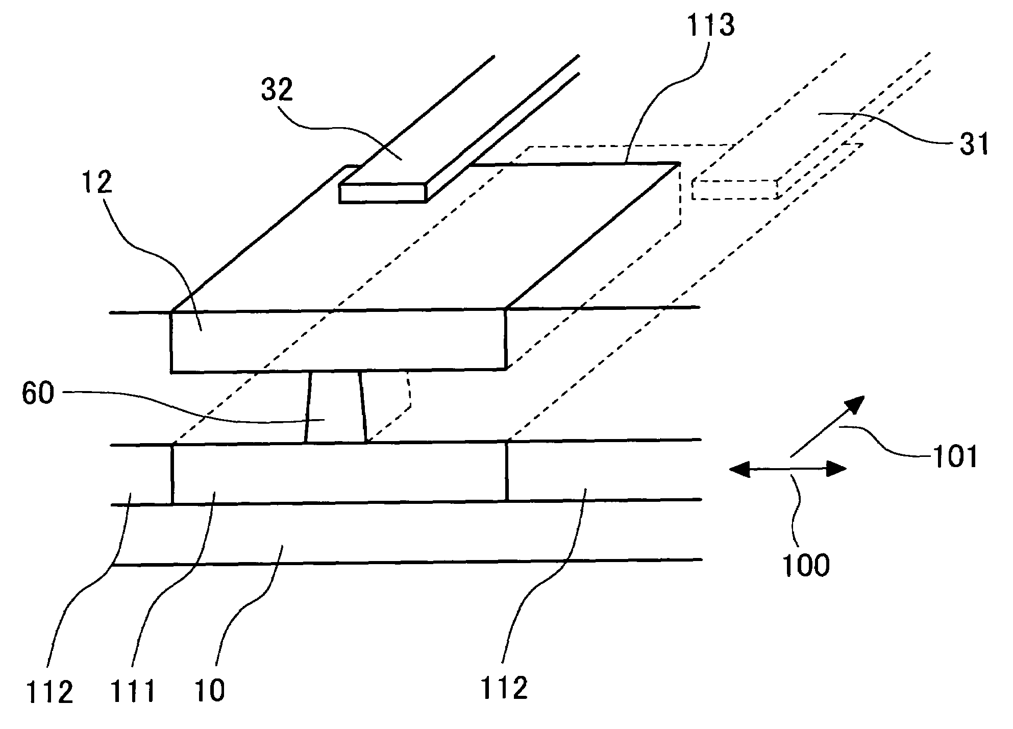
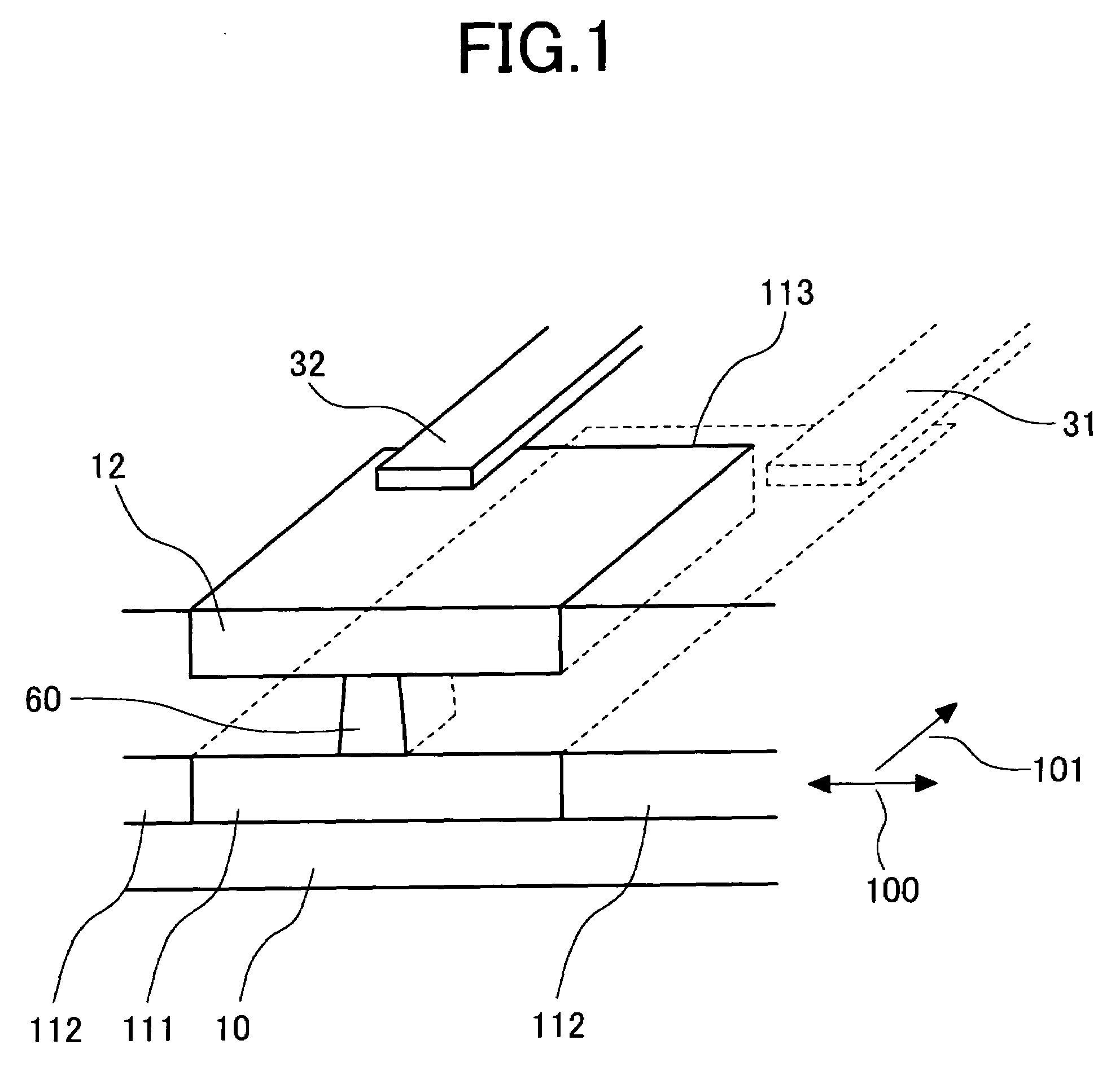
[0045]FIG. 1 shows an overhead view of a read head of a magnetoresistive head relating to the present invention. It is to be noted that FIG. 1 shows a status where a step for forming an upper shield layer and connecting a second lead line thereto has been completed. It is an overhead view from a plane on which a device is formed, into a stripe height direction, and even with the overhead view, portions which are invisible due to other layers are indicated with broken lines.
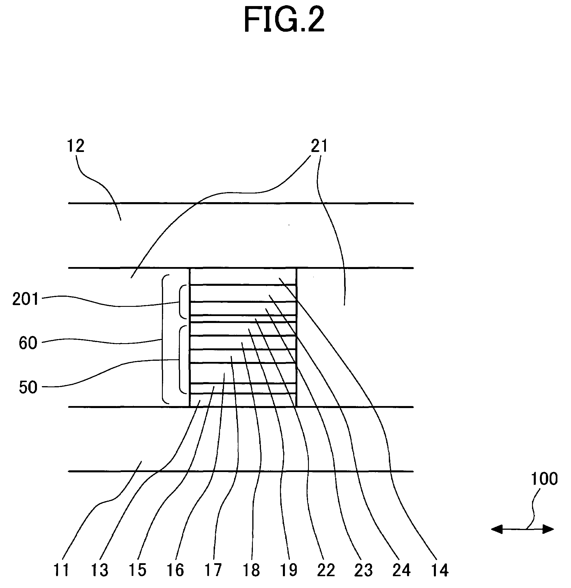
[0046]A film of Ni—Fe alloy is formed by plating on Al2O3—TiC substrate 10, whose surface has been coated with an insulating material such alumina, and then it is patterned to be a predetermined shape. Then, an alumina film is formed thereon and subjected to planarization by chemical mechanical polishing (CMP), so as to form a lower shield layer 111 and a lower alumina layer 112. A first lead line 31 is formed in such a manner as electrically connected with a back portion of the lower shield layer 111 in the strip...
example 2
[0060]FIG. 9 and FIG. 10 show a structure of a read head relating to another embodiment of the present invention. FIG. 9, in the left side, is a diagram looking down upon the read head from a plane where a magnetoresistive sensor is formed into a stripe height direction, and for explanation purpose, the upper shield layer 12 is cut off in the right side of FIG. 9, so as to clarify a positions of the lower shield layer 111 and the first lead line 31. FIG. 10 shows an arrangement of the shield layers and the lead lines, which is projected from the upper of the device fabricated plane onto a plane where the lower shield layer 111 is disposed.
[0061]As indicated in FIG. 9, at the edge parallel to the track width direction of the lower shield layer 111, a lead contact portion 113 having a width shorter than the length of the lower shield layer 111 in the track width direction is provided. At the lead contact portion 113, the first lead line 31 is electrically connected to the lower shield...
example 3
[0065]FIG. 11 is an overhead view of the read head portion of another embodiment of the present invention. In the right side of FIG. 11, the upper shield layer 12 is cut off, so as to clarify positions of the lower shield layer 111 and the first lead line 31. FIG. 12 shows an arrangement of the shield layers and the lead lines, which are projected from the upper of the device fabricated plane onto a plane where the lower shield layer 111 is disposed.
[0066]A structure of the present embodiment is that on the edge parallel to the track width direction of the upper shield layer 12, a lead contact portion 123 having a width shorter than the length of the upper shield layer 12 in the track width direction is provided. At the lead contact portion 123, the second lead line 32 is electrically connected with the upper shield layer 12. In this structure, even if a stress is acted on the upper shield layer 12 by disposing the lead line 32 on the upper shield layer 12, and a magnetic domain ori...
PUM
| Property | Measurement | Unit |
|---|---|---|
| length | aaaaa | aaaaa |
| height | aaaaa | aaaaa |
| width | aaaaa | aaaaa |
Abstract
Description
Claims
Application Information
 - R&D
- Intellectual Property
- Life Sciences
- Materials
- Tech Scout
- Unparalleled Data Quality
- Higher Quality Content
- 60% Fewer Hallucinations
Browse by: Latest US Patents, China's latest patents, Technical Efficacy Thesaurus, Application Domain, Technology Topic, Popular Technical Reports.
© 2025 PatSnap. All rights reserved.Legal|Privacy policy|Modern Slavery Act Transparency Statement|Sitemap|About US| Contact US: help@patsnap.com


