Transistor having multiple gate pads

a technology of transistors and gate pads, applied in the field of transistors with multiple gate pads, can solve the problems of gate shorting, inability to connect the sources of power mosfets internally, and high cost of all these approaches

Inactive Publication Date: 2005-11-08
ANALOG POWER INTPROP
View PDF16 Cites 9 Cited by
  • Summary
  • Abstract
  • Description
  • Claims
  • Application Information

AI Technical Summary

Problems solved by technology

Because the gate pads and source pads of the two dies are alternatively placed between gate and source, it does not allow the sources of the power MOSFETs to be connected internally.
This is because the alternating gate and source will cause the gate to be shorted to the source during wire bonding if the two sources are connected together internally.
All of these approaches may be relatively costly, as the manufacturing of the devices may be more complicate.

Method used


Image

  • Transistor having multiple gate pads
  • Transistor having multiple gate pads
  • Transistor having multiple gate pads

Examples


Embodiment Construction

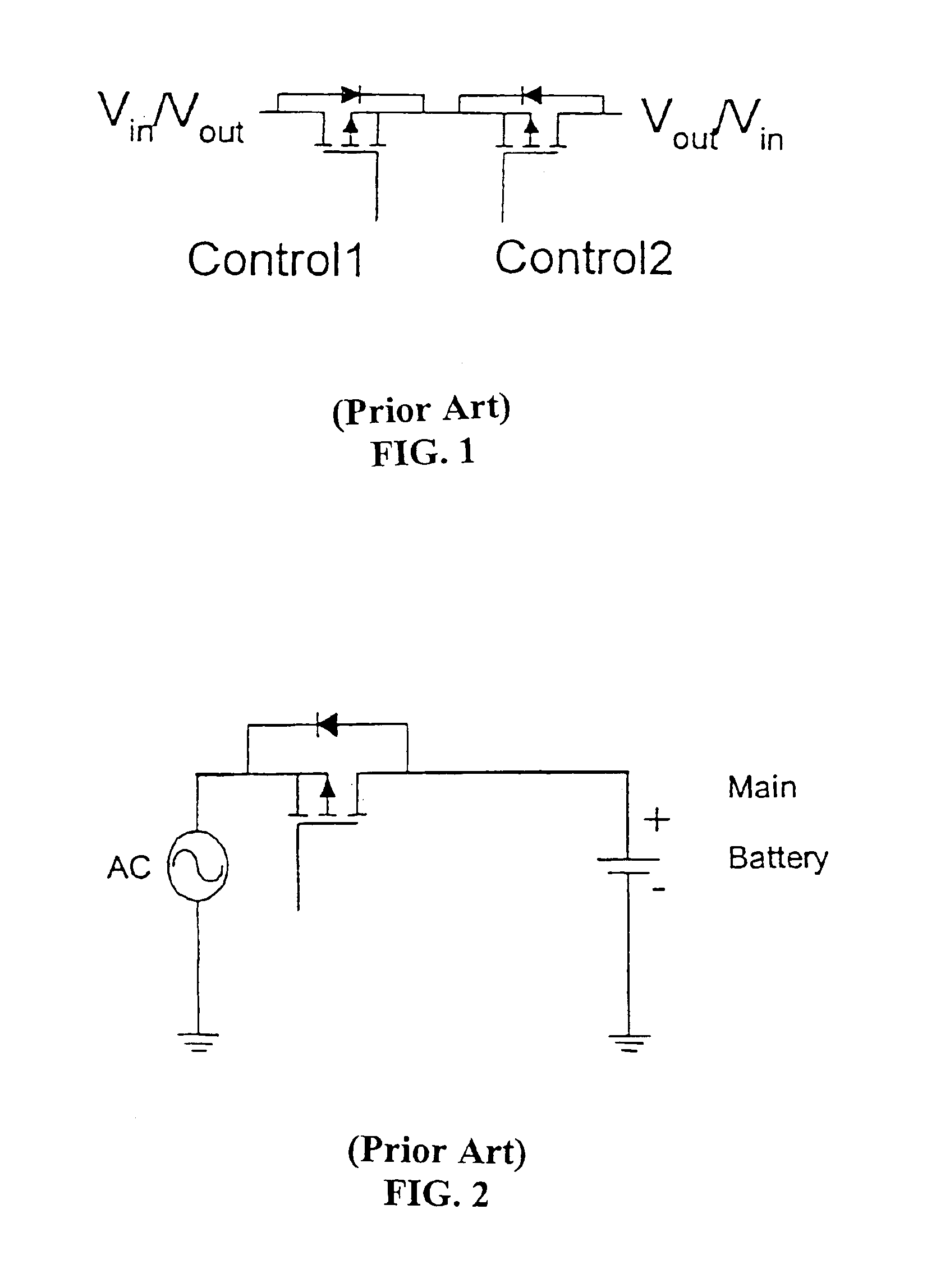
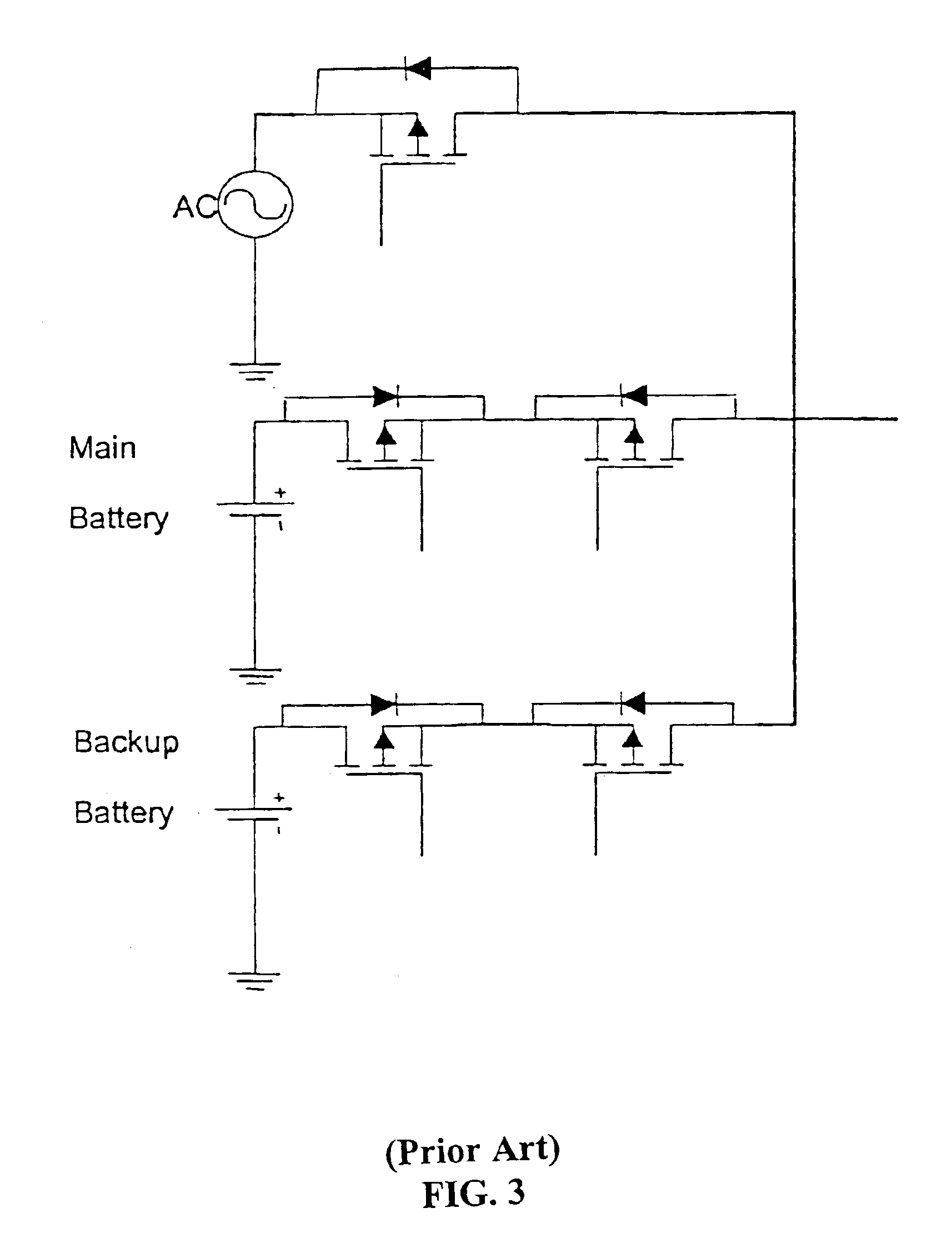
[0021]This invention is now described by way of example with reference to the figures in the following paragraphs. List 1 is a part list so that the reference numerals in the figures may be easily referred to.

[0022]Objects, features, and aspects of the present invention are disclosed in or are obvious from the following description. It is to be understood by one of ordinary skill in the art that the present discussion is a description of exemplary embodiments only, and is not intended as limiting the broader aspects of the present invention, which broader aspects are embodied in the exemplary constructions.

[0023]The following description assumes, for example, the above power MOSFETs as shown in FIG. 1 to FIG. 4 are contained in a single electronic package. A lead frame is generally defined as a piece of metal in a single electronic package, which carries at least one semiconductor component, such as a transistor, and provides leads for the semiconductor component to be connected wit...


PUM


Abstract

Current practice of the common source configuration is to connect the sources of the two discrete MOSFETs (housed either in separated packages or in a single package) externally on the printed circuit board. Because the gate pads and source pads of the two dies are alternatively placed between gate and source, it does not allow the sources of the power MOSFETs to be connected internally, which requires an additional layer of circuit board to connect the sources and the gates externally. This invention provides a novel electronic device layout design and a novel packaging technique for common source configuration, placing two MOSFETs in a package with their sources connected to a single source post which is located between tow gate posts. In order to facilitate gate bonding and to prevent any shorting between gate and source, two gate pads are used and placed at the upper adjacent corners of each MOSFET.

Description

FIELD OF THE INVENTION[0001]This invention relates to electronic devices involving at least one transistor and a lead frame, particularly those for switching multiple power sources.BACKGROUND OF THE INVENTION[0002]Power MOSFETs (Metal-Oxide-Semiconductor Field Effect Transistors) are commonly used in numerous applications, including power supplies, portable devices and automotive electronics. MOSFET is a type of three-terminal transistor having a gate, a source and a drain terminal. One of the tasks of the power MOSFETs in these applications is to provide switching function and control the power delivery from the source to the load. One of the most popular applications of the power MOSFETs is for switching multiple power sources in notebook computers. In this case, a common source configuration of two power MOSFETs, as shown in FIG. 1 is required. The two power MOSFETs are basically connected back to back with the sources connected together.[0003]In a typical notebook power supply s...

Claims


Application Information

Patent Timeline
Patent Type & Authority Patents(United States)
IPC IPC(8): H01L23/495H01L23/48H01L23/485
CPCH01L23/49541H01L23/49562H01L24/05H01L24/48H01L24/49H01L2224/04042H01L2224/05556H01L2224/05599H01L2224/48227H01L2224/48247H01L2224/48463H01L2224/48472H01L2224/49111H01L2224/49171H01L2224/49175H01L2224/85399H01L2924/01033H01L2924/01082H01L2924/13091H01L2924/00014H01L2924/00H01L2224/0603H01L2224/48465H01L2224/45099H01L2924/00012H01L2224/05552H01L2224/45015H01L2924/207
Inventor SIN, JOHNNY KIN-ONLIU, MINGLAI, TOMMY MAU-LAU
Owner ANALOG POWER INTPROP
Why Eureka
Try Eureka