
Synchronous memory device for preventing erroneous operation due to DQS ripple

a synchronous memory and ripple technology, applied in the field of synchronous memory devices, can solve the problems that the data access scheme used in the conventional synchronous memory devices cannot be used for the ddr memory devices, and the sdr synchronous memory devices are also short, so as to prevent erroneous operations

Inactive Publication Date: 2005-09-27
SK HYNIX INC
View PDF6 Cites 34 Cited by
  • Summary
  • Abstract
  • Description
  • Claims
  • Application Information

AI Technical Summary

Benefits of technology

[0032]It is, therefore, an object of the present invention to provide a memory device capable of preventing erroneous operation due to DQS ripple.

Problems solved by technology

However, the SDR synchronous memory device is also short to satisfy system speed for high-speed operation.
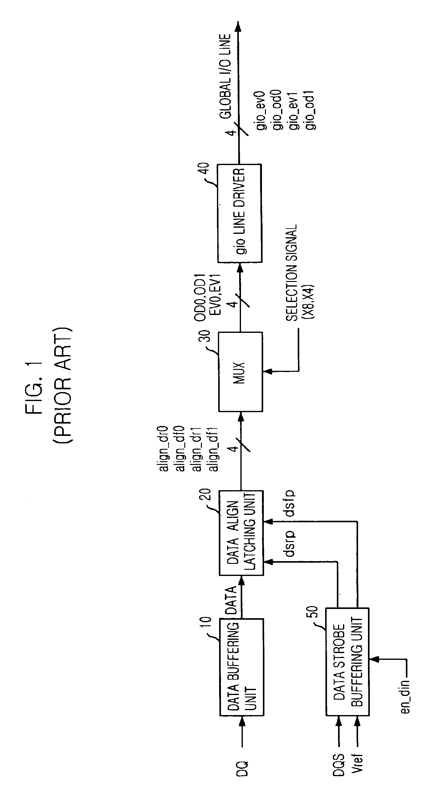
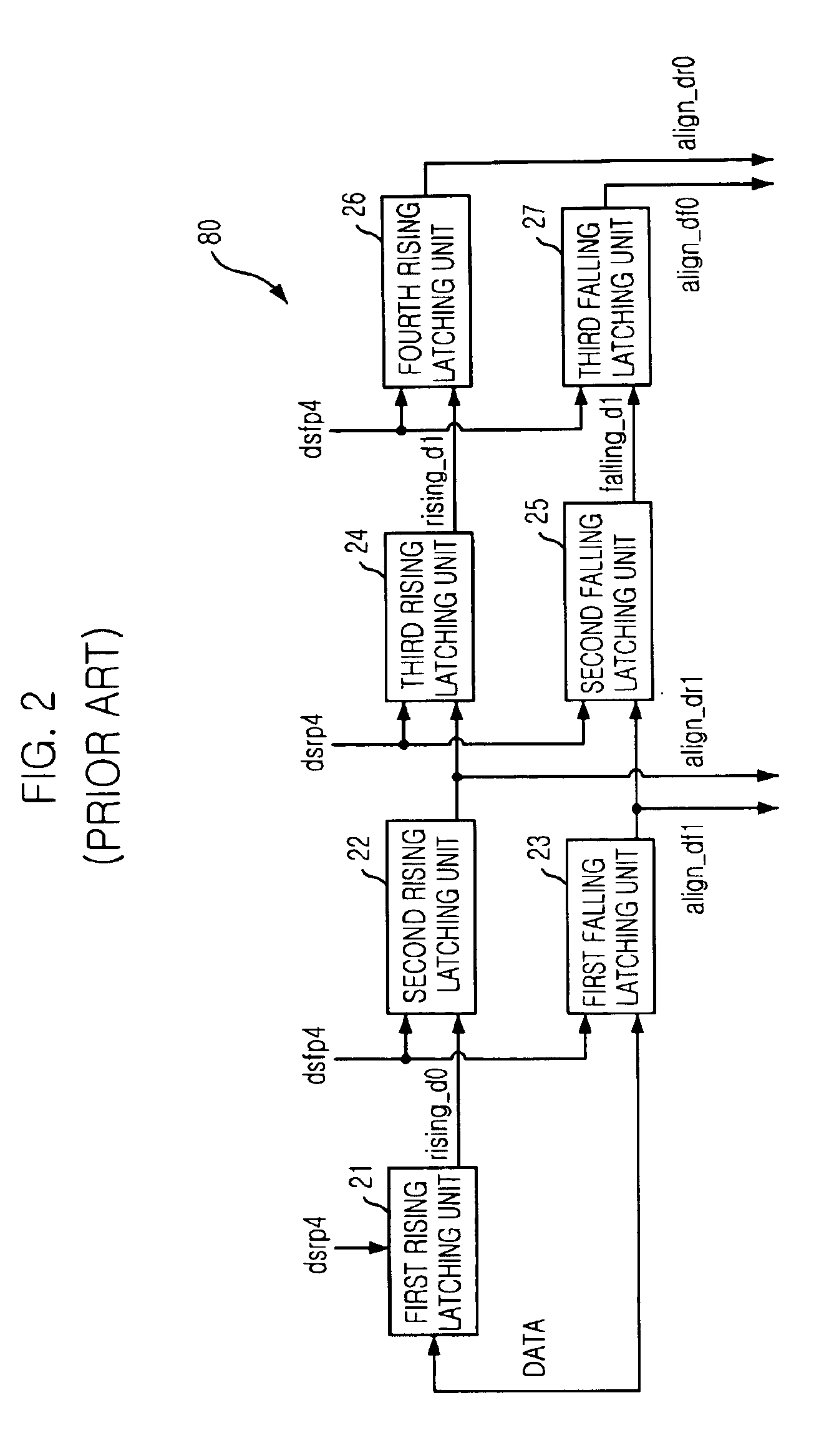
However, because the DDR memory device should output or input two data for one clock cycle, in order to perform these data input and output effectively, the data access scheme that is used in the conventional synchronous memory device cannot be used for the DDR memory device.
However, during return to the high impedance state after input of all the data, ripple happens, which is to cause error because of overshoot of the ripple.

Method used


Image

  • Synchronous memory device for preventing erroneous operation due to DQS ripple
  • Synchronous memory device for preventing erroneous operation due to DQS ripple
  • Synchronous memory device for preventing erroneous operation due to DQS ripple

Examples


Embodiment Construction

[0051]Hereinafter, with reference to the accompanying drawings, a preferred embodiment of the present invention will be explained in detail.

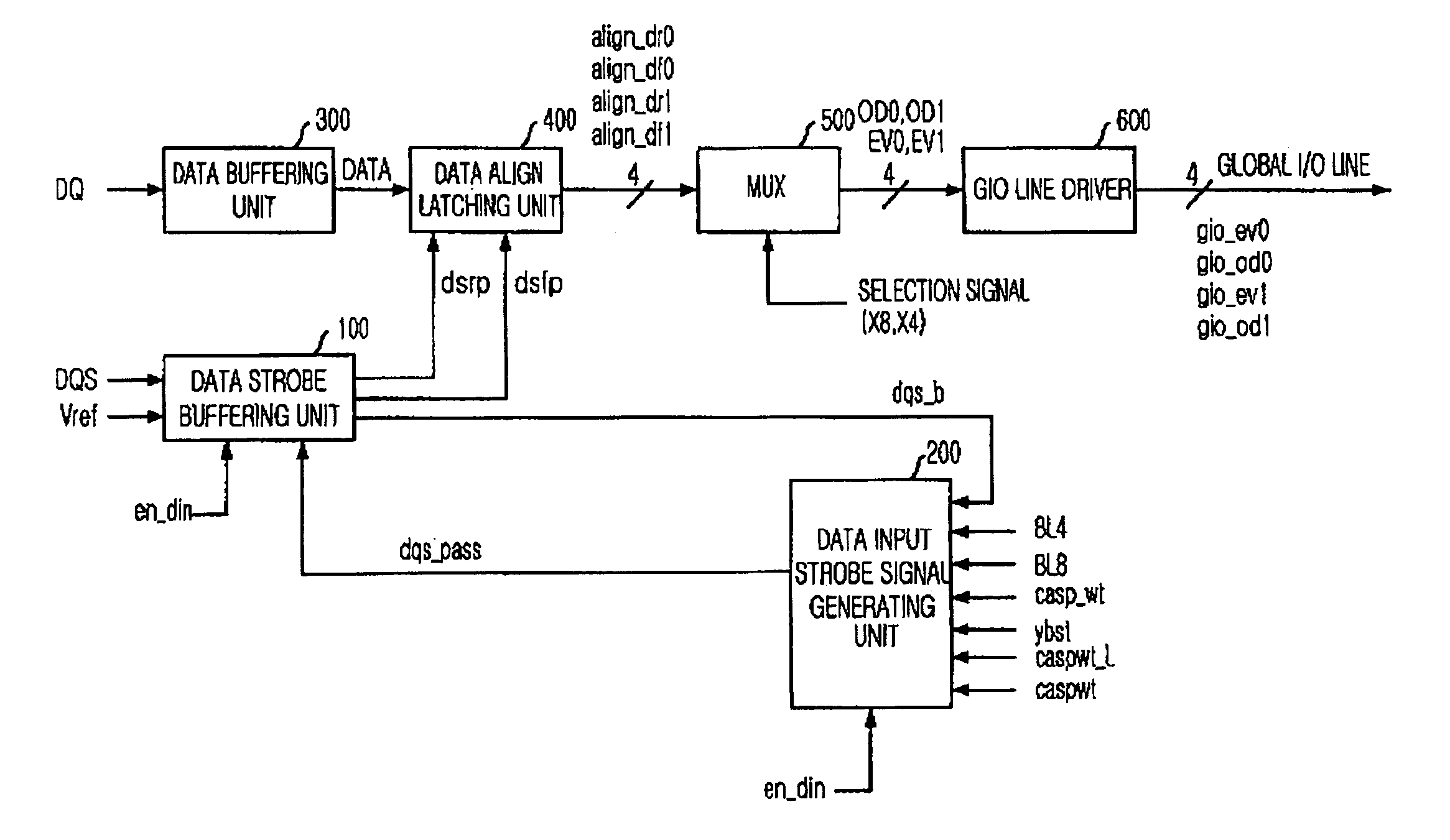
[0052]FIG. 6 is a block diagram of a synchronous memory device in accordance with a preferred embodiment of the present invention.

[0053]Referring to FIG. 6, there is provided a synchronous memory device receiving a number of data in synchronous with a rising edge and a falling edge of an operation clock in accordance with an embodiment of the present invention, comprising a data strobe buffering unit 100 for outputting a rising pulse dsrp and a falling pulse dsfp for detecting a rising edge and a falling edge of a DQS signal that is clocked when data is inputted while sustaining high impedance state when there is no operation, a data align latching unit 400 for latching and aligning the data in synchronous with the rising pulse dsrp and the falling pulse dsfp, and a DQS signal controlling unit 200 for controlling the data strobe buffering unit t...


PUM


Abstract

A synchronous memory device, receiving a number of data in synchronization with a rising edge and a falling edge of a clock, includes a data strobe buffering unit, a data align latching unit and a DQS signal controlling unit. The data strobe buffering unit outputs a rising pulse and a falling pulse for detecting a rising edge and a falling edge of a DQS signal that sustains a high impedance state when there is no operation and is clocked while the data is inputted. The data align latching unit latches and aligns the data in synchronization with the rising pulse and the falling pulse. The DQS signal controlling unit controls the data strobe buffering unit to output the rising pulse and the falling pulse to the data align latching unit only when the DQS signal is clocked.

Description

FIELD OF THE INVENTION[0001]The present invention relates to semiconductor memory devices; and, more particularly, to a semiconductor memory device capable of preventing erroneous operation due to DOS ripple that is clocked and inputted at the timing when data is inputted.BACKGROUND OF THE INVENTION[0002]A semiconductor memory device has been continuously improved in its integrated degree and its operation speed. For rising the operating speed, so called, a synchronous memory device is introduced, which operates in synchronous with a clock from external of a memory chip.[0003]The first suggested one is so called a SDR (Single Data Rate) synchronous memory device, which inputs or outputs one data over one clock cycle at a data pin in synchronous with a rising edge of the clock from the external of the memory device.[0004]However, the SDR synchronous memory device is also short to satisfy system speed for high-speed operation. Therefore, a DDR (Double Data Rate) synchronous memory dev...

Claims


Application Information

Patent Timeline
Patent Type & Authority Patents(United States)
IPC IPC(8): G11C8/00G11C11/40G11C7/10G11C7/22
CPCG11C7/1066G11C7/1078G11C7/1087G11C7/1093G11C7/22G11C11/40
Inventor LEE, SANG-HEE
Owner SK HYNIX INC
Learn More