LCD and method of manufacture thereof

a liquid crystal device and manufacturing method technology, applied in non-linear optics, instruments, optics, etc., can solve problems such as lowering sealing strength and occurrence of breaking defects, and achieve the effect of accurate confirmation of position

Inactive Publication Date: 2005-08-16
BOE TECH GRP CO LTD
View PDF7 Cites 35 Cited by
  • Summary
  • Abstract
  • Description
  • Claims
  • Application Information

AI Technical Summary

Benefits of technology

[0039]In addition, it is preferable in accurately confirming the position of the sealing material or the anisotropic conductive material that all of the alignment mark be substantially superimposed on the end of the sealing material or the anisotropic conductive material.
[0040]Furthermore, the end of the sealing material and the end of the anisotropic conductive material may preferably be formed in the same shape so as to be superimposed each other when the substrates are bonded to each other. The end of the sealing material and the end of the anisotropic conductive material joined to each other are formed in the same shape, whereby formation of air bubbles in the sealing section in the joined area, or occurrence of sealing defects can be prevented even if the slight displacement of the position of the sealing material relative to the position of the anisotropic conductive material occurs.

Problems solved by technology

In addition, in the above conventional liquid crystal device, when the sealing material on one substrate and the anisotropic conductive material on the other substrate are joined to each other when the substrates are bonded to each other, displacement of the sealing material relative to the anisotropic conductive material, and sealing defects due to insufficient sealing material or insufficient anisotropic conductive material may occur in joined areas between the sealing material and the anisotropic conductive material, or air bubbles may become entrapped into the joined areas lowering sealing strength.
When the sealing section protrudes to the outside of the joined areas due to an excess of the sealing material in this way, in a substrate breaking process to be performed later (a process in which large substrates (base substrates) are bonded to each other to form a plurality of liquid crystal panels at one time, scribe lines are formed on the surface of the large base substrates, and stress is applied along the scribe lines to break the large base substrates), breaking defects may occur when the applied stress is uneven, whereby a broken-off section is formed at a site not along the scribe lines.

Method used


Image

  • LCD and method of manufacture thereof
  • LCD and method of manufacture thereof
  • LCD and method of manufacture thereof

Examples


Embodiment Construction

[0058]Description will now be given of a preferred mode for carrying out the invention.

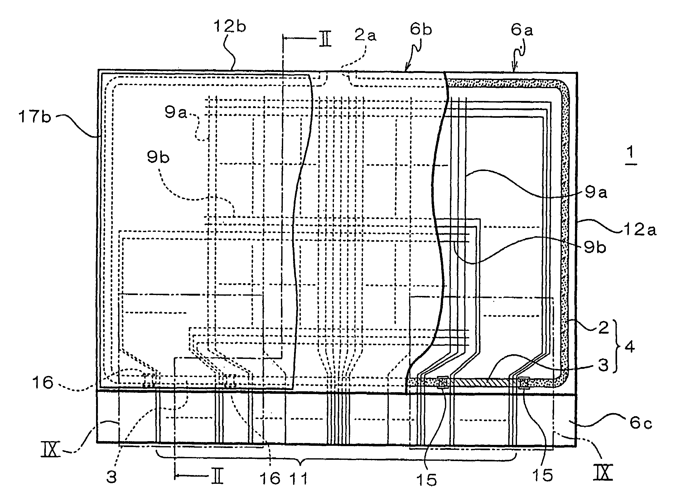
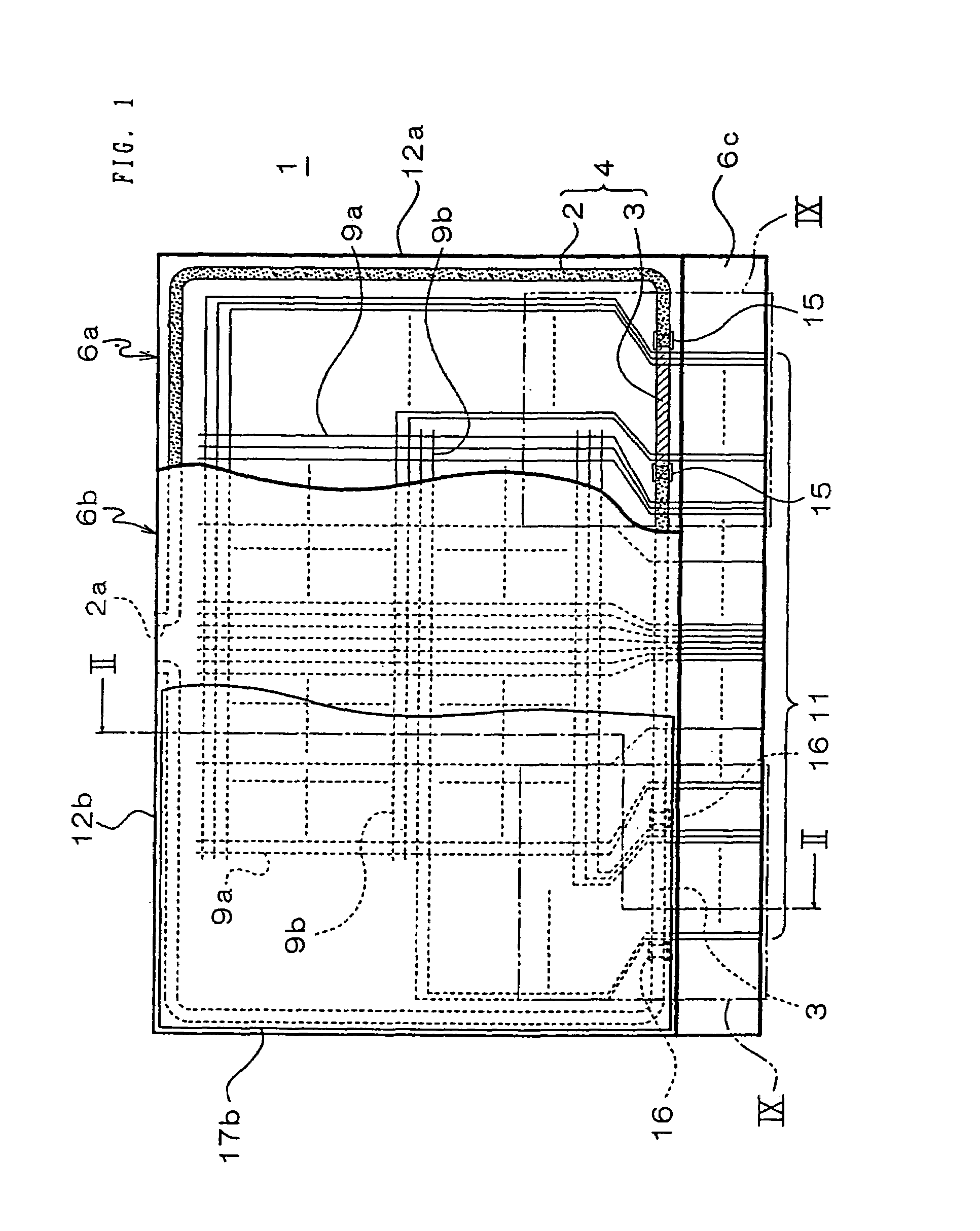
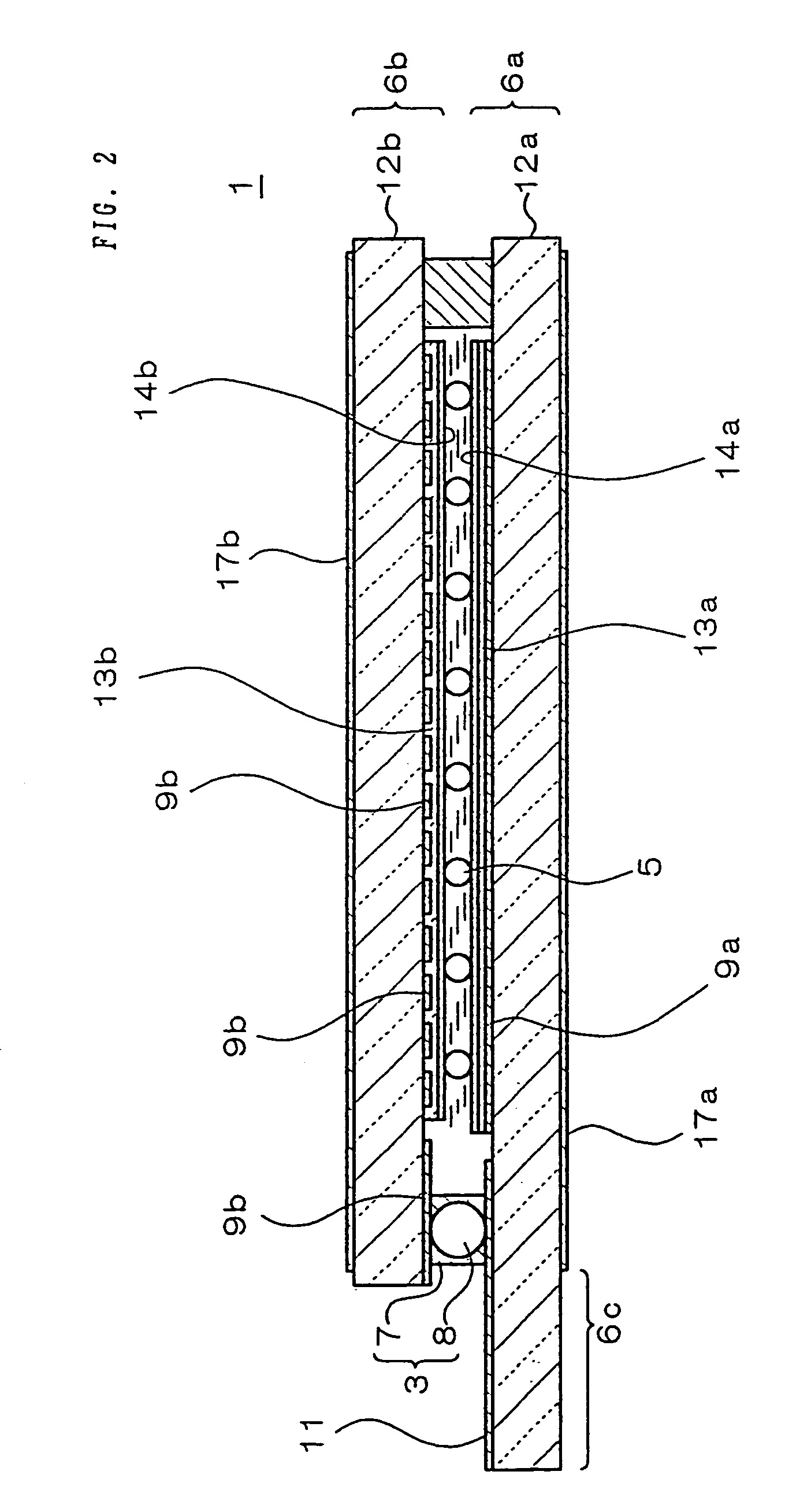
[0059]FIG. 1 shows a liquid crystal panel 1 that is a principal part of a liquid crystal device of an embodiment according to the present invention. FIG. 2 shows a panel structure of the liquid crystal panel 1 by a section taken along the line II—II in FIG. 1. The liquid crystal device of this embodiment are formed by attaching an illuminating device, such as a backlight, for illuminating the liquid crystal panel from behind, a liquid crystal driving circuit, such as a liquid crystal-driving IC, for driving the liquid crystal panel, a conductive-connecting member, such as a flexible printed circuit board, for conductive-connecting the liquid crystal panel to the outside, and other various types of additional devices to the liquid crystal panel 1.

[0060]The liquid crystal panel 1 includes a cell structure such that a sealing material 2 and an anisotropic conductive material 3 are joined so as to be ...


PUM

PropertyMeasurementUnit
conductiveaaaaaaaaaa
anisotropic conductiveaaaaaaaaaa
widthaaaaaaaaaa

Abstract

The present invention provides a manufacturing method or a structure capable of reducing occurrence of sealing defects and breaking defects by resolving defects in form of a joined area between a sealing material and an anisotropic conductive material. A sealing material (2) is formed in such a manner as to superimpose ends (2b) on alignment marks (15) formed on the surface of a first substrate (6a), an anisotropic conductive material is formed in such a manner as to superimpose ends 3b on alignment marks (16) formed on the surface of a second substrate (6b), and the sealing material 2 and the anisotropic conductive material (3) are joined by bonding the first substrate (6a) and the second substrate (6b) to form one-piece sealing section (4).

Description

BACKGROUND OF THE INVENTION[0001]1. Technical Field[0002]The present invention relates to a liquid crystal device suitably used for displaying images, such as letters, numeric characters, and pictures, by controlling the orientation of liquid crystals sealed between a pair of substrates. The present invention also relates to a method for manufacturing the liquid crystal device.[0003]2. Background Art[0004]In general, liquid crystal devices are formed by attaching an illuminating device, such as a backlight, and a liquid crystal-driving IC to a liquid crystal panel. The liquid crystal panel is formed by bonding a pair of substrates formed with electrodes across a sealing section so that the electrodes oppose each other, by sealing liquid crystal in a cell gap formed between the electrodes, and by bonding polarizers on the outside surfaces of the substrates.[0005]One of the pair of substrates may be provided with a substrate protrusion protruding toward the outer periphery from the ot...

Claims


Application Information

Patent Timeline
Patent Type & Authority Patents(United States)
IPC IPC(8): G02F1/13G02F1/1339G02F1/1333G02F1/1345
CPCG02F1/1339G02F2001/133354G02F2001/13456G02F1/133354G02F1/13456
Inventor MIYAZAKI, TAKASHINAKAHARA, HIROKI
Owner BOE TECH GRP CO LTD
Why Eureka
Try Eureka