
Light emitting element and manufacturing method for the same

a technology of light-emitting elements and manufacturing methods, which is applied in the direction of semiconductor/solid-state device manufacturing, electrical equipment, semiconductor devices, etc., can solve the problems of difficult to form such a layer having the continuously changing refractive index on the surface of led, poor extraction efficiency of led chips encapsulated with epoxy resin, and difficult to say that an inherent property

Inactive Publication Date: 2005-08-02
KK TOSHIBA
View PDF5 Cites 18 Cited by
  • Summary
  • Abstract
  • Description
  • Claims
  • Application Information

AI Technical Summary

Benefits of technology

The present invention relates to a light emitting element and a manufacturing method thereof. The light emitting element has a layer of light emitting material sandwiched between two parallel surfaces and four rough side surfaces. The manufacturing method involves making cuts on the substrate and separating it into chips, followed by a wet etching process to form rough surfaces on the chip's side surfaces. The technical effects of this invention include improved light emitting efficiency and stability, as well as simplified manufacturing process.

Problems solved by technology

Accordingly, the extraction efficiency for the LED chip encapsuled with the epoxy resin may become poor.
In fact, it is difficult to form such a layer having the continuously changing refractive index on the surfaces of the LED.
As described above, by tilting and roughening the side surfaces of the LED it is possible to improve the extraction efficiency, however the following new problems arise
Therefore it is difficult to say that an inherent property of the internal quantum efficiency of the light emitting layer is sufficiently exhibited.
(2) Reliability for the LED chip may be decreased due to a nonuniform stress of the molded resin.
Such nonuniform stress exerted on the LED chip causes strain and cracks, as well as a remarkable loss in the long-term reliability of the LED chip.
In addition, excessive stress on the LED chip causes peeling and breakage of the LED chip.
While in rectangular solid LED chips the stresses with the molded resin are balanced out by canceling the stresses applied to opposite side surfaces, since shape symmetry cannot be assured, the stresses generated with the molded resin are extremely difficult to thoroughly eliminate in a trapezoidal LED chip.

Method used


Image

  • Light emitting element and manufacturing method for the same
  • Light emitting element and manufacturing method for the same
  • Light emitting element and manufacturing method for the same

Examples


first embodiment

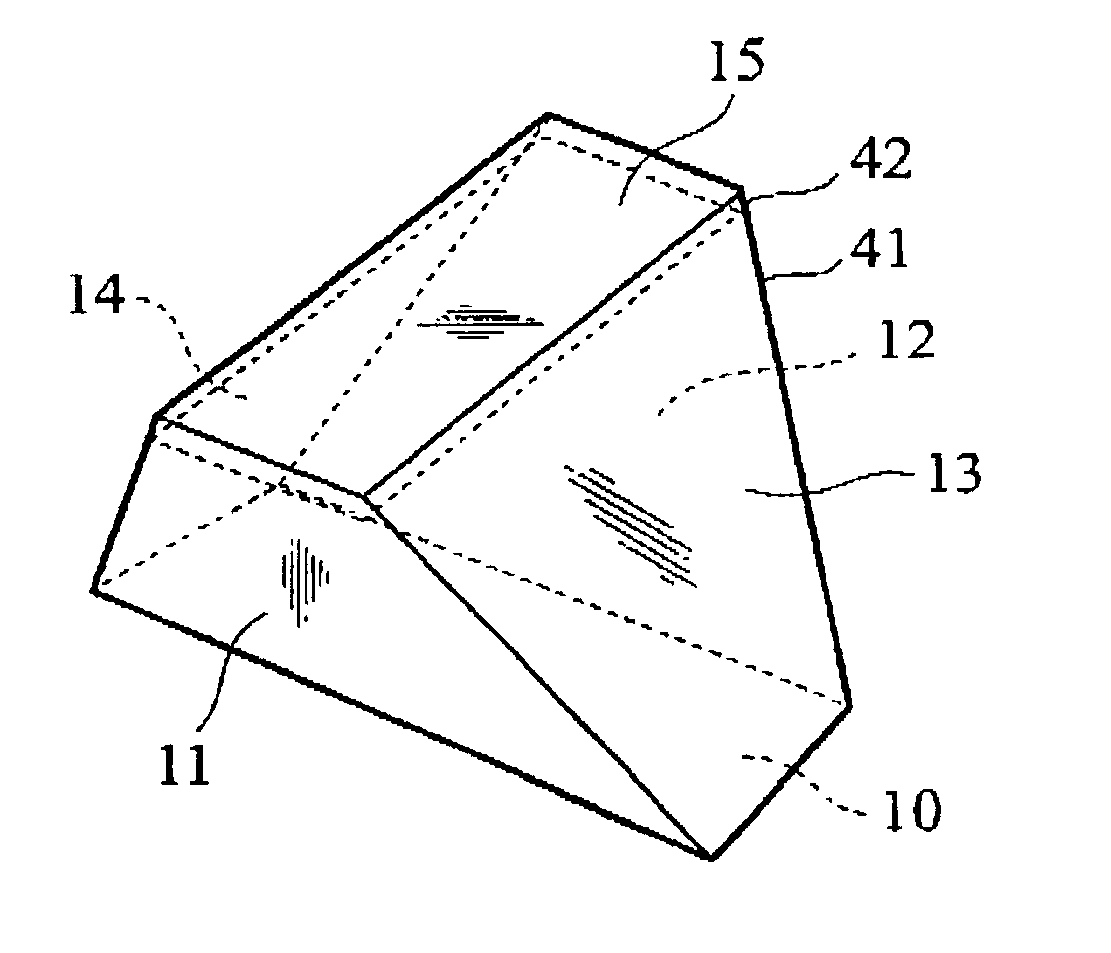
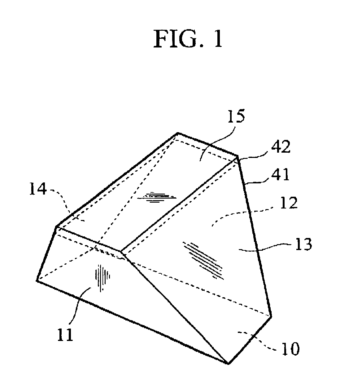
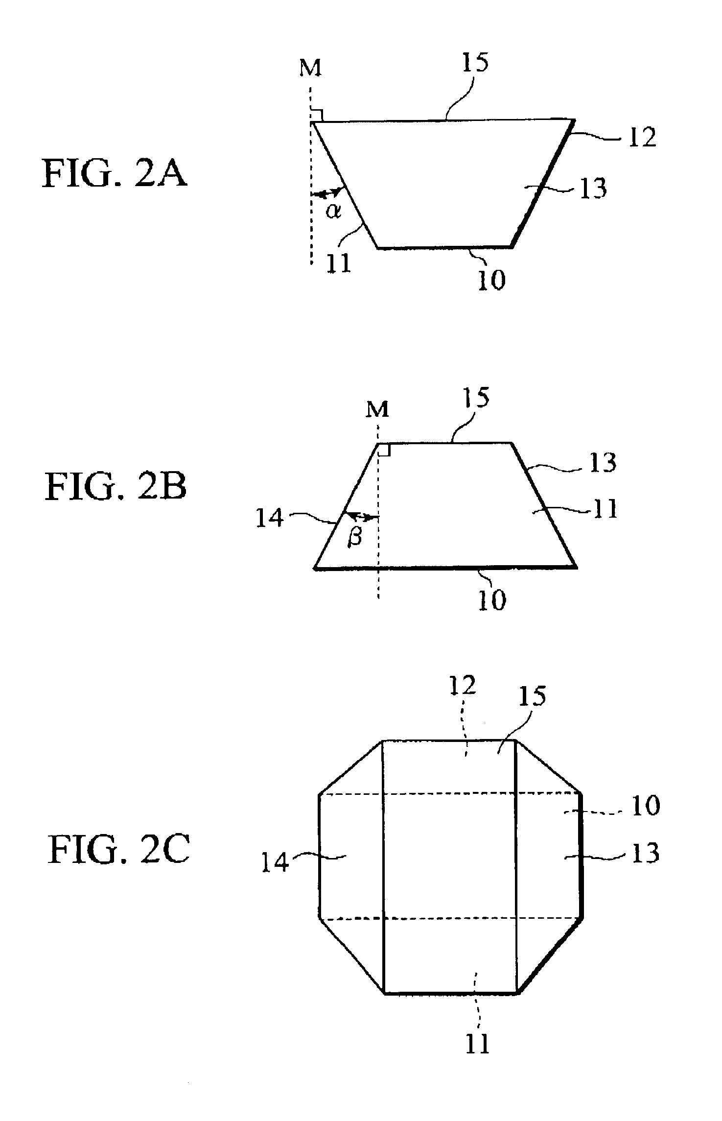
[0031]A light emitting element chip (LED chip) according to a first embodiment of the present invention, as shown in FIG. 1 as an oblique perspective view, FIGS. 2A and 2B as side views, and FIG. 2C as a top view, has a hexahedron shape. The LED chip is fabricated, for example, from an LED wafer (semiconductor substrate) with a thickness of about 150 μm, by using GaP for a base substrate 41 and InGaAlP for a light emitting layer 42. The hexahedral LED chip includes a rectangular top surface (first principal surface) 15 having, e.g. a long edge of 300 μm and a short edge of 160 μm, a rectangular bottom surface (second principal surface) 10 having, e.g. a long edge of 300 μm and a short edge of 160 μm, and first through fourth side surfaces 11, 12, 13, and 14. The long edges of the top and bottom surfaces are arranged orthogonal to each other. In addition, the first and second side surfaces 11 and 12 facing to each other are formed by trapezoids having the same shape and dimensions an...

second embodiment

[0073]An LED chip 148 according to a second embodiment of the present invention, as shown in FIG. 11, has InGaAlP epitaxial layers including a light emitting layer disposed on a GaP substrate as a base substrate. The base substrate includes the GaP substrate 108 having a p-type conductivity and a p-type GaP layer 107 disposed on the GaP substrate 108. The InGaAlP epitaxial layers includes an n-type current diffusion layer 102, an n-type clad layer 103, an active layer 104, a p-type clad layer 105, and a bonding layer 106. A light emitting layer is the active layer 104 sandwiched between the n-type clad layer 103 and the p-type clad layer 105. The bonding layer 106 of the epitaxial layer is disposed directly on the p-type GaP layer 107 of the base substrate. First and second electrodes 109 and 110 of the LED chip 148 are provided on a bottom surface of the GaP substrate 108 and a top surface of the n-type current diffusion layer 102. The base substrate has rough surface 111 on side s...


PUM


Abstract

A light emitting element includes: a light emitting layer; a rectangular first principal surface being parallel to the light emitting layer; a rectangular second principal surface opposing to the first principal surface so that the light emitting layer is sandwiched between the first and second principal surfaces; and first through fourth side surfaces of the light emitting element provided with a rough surface, the first through fourth side surfaces connecting between the first principal surface and the second principal surface, respectively so as to define a solid shape.

Description

CROSS REFERENCE TO RELATED APPLICATIONS[0001]This application is based upon and claims the benefit of priority from prior Japanese Patent Application P2002-20185 filed on Jan. 29, 2002 and Japanese Patent Application P2003-16275 filed on Jan. 24, 2003; the entire contents of which are incorporated by reference herein.BACKGROUND OF THE INVENTION[0002]1. Field of the Invention[0003]The present invention relates to a light emitting element having a high level of brightness and a manufacturing method for the same.[0004]2. Description of the Related Art[0005]An optical power output of a semiconductor light emitting element (LED) is determined by a product of an internal quantum efficiency representing a conversion efficiency of an injection current to photons, and an extraction efficiency for the photons emitted from the semiconductor passing through a molded resin or air. In order to improve the extraction efficiency and increase the optical power output of the LED, many methods have be...

Claims


Application Information

Patent Timeline
Patent Type & Authority Patents(United States)
IPC IPC(8): H01L33/00H01L21/301H01L21/306H01L33/16H01L33/22H01L33/30
CPCH01L33/20
Inventor AKAIKE, YASUHIKOWASHIZUKA, SHOICHIKINUGAWA, YOSHIYUKI
Owner KK TOSHIBA
Learn More