Method and structure for determining a concentration profile of an impurity within a semiconductor layer

a technology of impurity concentration and semiconductor layer, applied in the direction of semiconductor/solid-state device testing/measurement, semiconductor/solid-state device details, instruments, etc., can solve the problems of reducing production efficiency and device quality, difficult to find an analytical technique suitable for use in semiconductor fabrication, and large equipment pieces, etc., to achieve accurate and timely manner, reduce process cycle time, and increase production efficiency

Inactive Publication Date: 2005-06-14
MONTEREY RES LLC
View PDF9 Cites 4 Cited by
  • Summary
  • Abstract
  • Description
  • Claims
  • Application Information

AI Technical Summary

Benefits of technology

[0014]There may be several advantages to determining the concentration of an impurity within a layer using the method and structure described herein. For example, the method and structure described herein may offer a manner with which to analyze the impurity concentration of a thin film of a semiconductor device in an accurate and timely manner. In particular, the method described herein may determine an impurity concentration of a thin film within a semiconductor fabrication area in less than approximately one hour. Such a method may be particularly advantageous over the conventional method of sending samples to an outside testing facility and waiting days or weeks for the results. As such, process cycle time may be decreased, thereby increasing production efficiency. In addition, the method described herein may advantageously reduce fabrication costs. In particular, outside testing fees and / or expensive equipment used for in-house analysis do not have to be expensed or purchased, thereby decreasing fabrication costs.

Problems solved by technology

Inaccurate analysis of one or more process parameters within the fabrication of a semiconductor device, such as a transistor, may hinder or prohibit the function of the device, leading to a reduction in production efficiency and device quality.
At present, it is difficult to find an analytical technique suitable for use in semiconductor fabrication that can characterize the composition of a thin film in a simple, accurate, and cost-effective manner.
Many current techniques require large pieces of equipment, such as spectrometers that are not used within a fabrication area due to size and cleanliness requirements.
In addition, current techniques typically employ expensive equipment, thereby increasing the fabrication cost of the semiconductor devices.
As a result, production throughput and efficiency is sacrificed due to the increased process cycle time of the devices.

Method used


Image

  • Method and structure for determining a concentration profile of an impurity within a semiconductor layer
  • Method and structure for determining a concentration profile of an impurity within a semiconductor layer
  • Method and structure for determining a concentration profile of an impurity within a semiconductor layer

Examples


Embodiment Construction

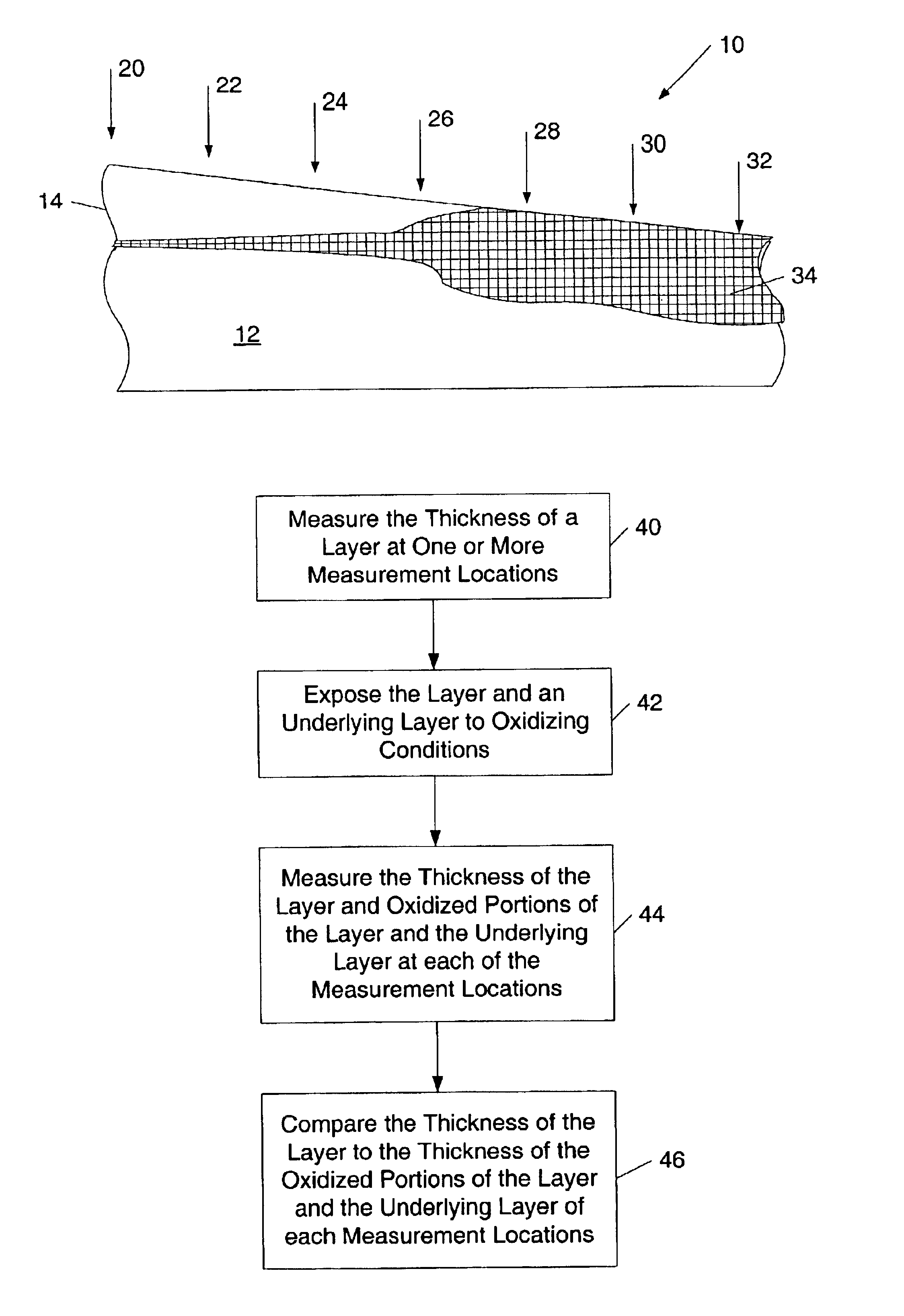
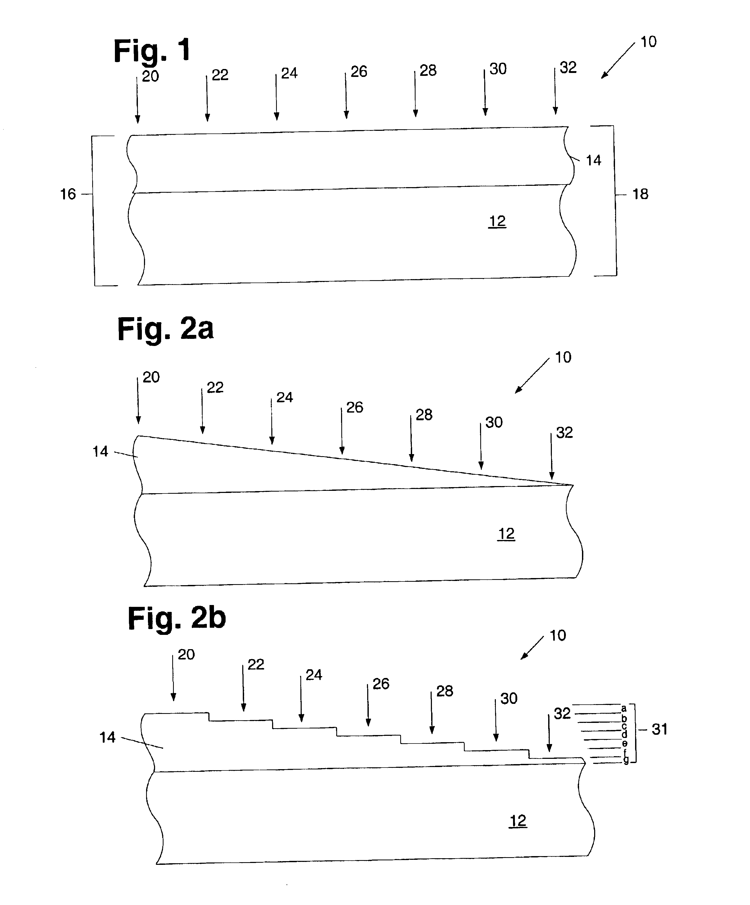
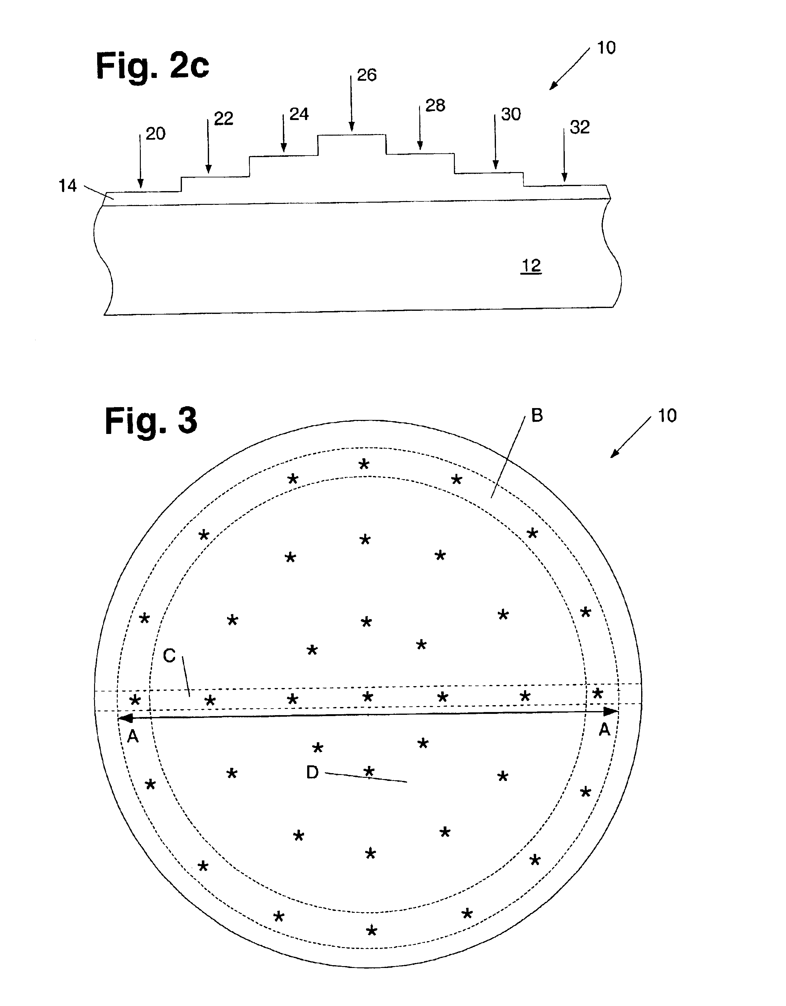
[0026]Turning to the drawings, exemplary embodiments of a method for measuring a concentration of an impurity within a layer of a semiconductor topography is shown in FIGS. 1-7. Moreover, FIGS. 1-7 illustrate a method for determining a concentration profile of an impurity within such a layer. In general, the arrangement of impurities within a material may differ. In particular, one or more portions of a layer may include higher concentrations of an impurity than other portions of the layer. The method described herein offers a technique by which to determine the concentration of an impurity within a particular location of a layer. In addition or alternatively, the method described herein may be used to determine the concentration profile of an impurity within a layer with a graded refractive index. In general, an impurity may refer to any species deliberately introduced into a material. In a preferred embodiment of the method described herein, the impurity may include any species ad...


PUM


Abstract

A method is provided for determining a concentration profile of an impurity within a layer of a semiconductor topography. The method may include exposing the layer and an underlying layer to oxidizing conditions. In addition, the method may include comparing thickness measurements of total dielectric above the underlying layer taken before and after exposing the topography to oxidizing conditions . In some cases, the comparison may include plotting pre-oxidation thickness measurements versus post-oxidation measurements. In other embodiments, the comparison may include determining differences between the pre-oxidation and post-oxidation thickness measurements and correlating the differences to concentrations of the impurity. In some cases, such a correlation may include subtracting a concentration of the impurity at a first location along the semiconductor topography from a concentration of the impurity at a second location along the semiconductor topography.

Description

CROSS-REFERENCE TO RELATED APPLICATIONS[0001]This application is a continuation in part of Ser. No. 10 / 023,065, filed Dec. 17, 2001, now U.S. Pat. No. 6,664,120.BACKGROUND OF THE INVENTION[0002]1. Field of the Invention[0003]This invention relates to determining material composition, and more particularly to a method and a structure for determining one or more component concentrations contained in a material. 2. Description of the Related Art[0004]The following descriptions and examples are not admitted to be prior art by virtue of their inclusion within this section.[0005]Compositional analysis of materials is desirable for many applications. For example, the type of adhesive applied to a tape product or the type of metal or paint applied to a product for corrosion protection is critical for the functionality of the products. The method and structure described herein are discussed primarily with respect to the analysis of thin films within semiconductor devices. The term “thin film...

Claims


Application Information

Patent Timeline
IPC IPC(8): G01N19/06G01N19/00G01N1/32H01L23/544H01L21/66
CPCH01L22/20G01N1/32H01L22/34G01N19/06
Inventor NARAYANAN, SUNDARRAMKUMAR, KRISHNASWAMY
Owner MONTEREY RES LLC
Why Eureka
Try Eureka