Eureka AIR delivers breakthrough ideas for toughest innovation challenges, trusted by R&D personnel around the world.

Three-dimensional photonic crystal waveguide structure and method

a waveguide and three-dimensional technology, applied in the field of waveguides, can solve the problems of limited practical interest, difficult to form 3d photonic crystal waveguides, and the band gap of photonic crystals in the microwave range of the spectrum, and achieve the effect of adding another level of complexity to the 3d waveguides of such crystals

Inactive Publication Date: 2005-05-24
MICRON TECH INC
View PDF76 Cites 60 Cited by
  • Summary
  • Abstract
  • Description
  • Claims
  • Application Information

AI Technical Summary

Problems solved by technology

This photonic crystal has a bandgap in the microwave range of the spectrum and is of limited practical interest.
To date, however, readily forming 3D photonic crystals waveguides has proven difficult.
While some techniques have been developed for fabricating 3D photonic crystals, they involve extreme process conditions, such as forming individual dielectric layers and then stacking and bonding the layers to build the crystal.
The formation of 3D waveguides in such crystals adds yet another level of complexity.

Method used

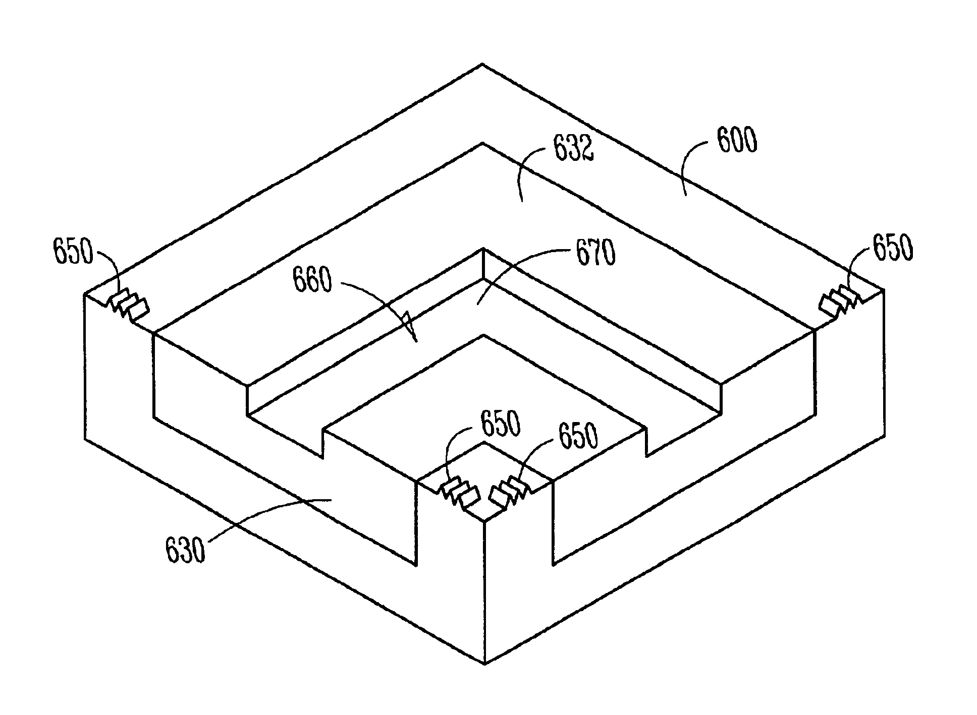
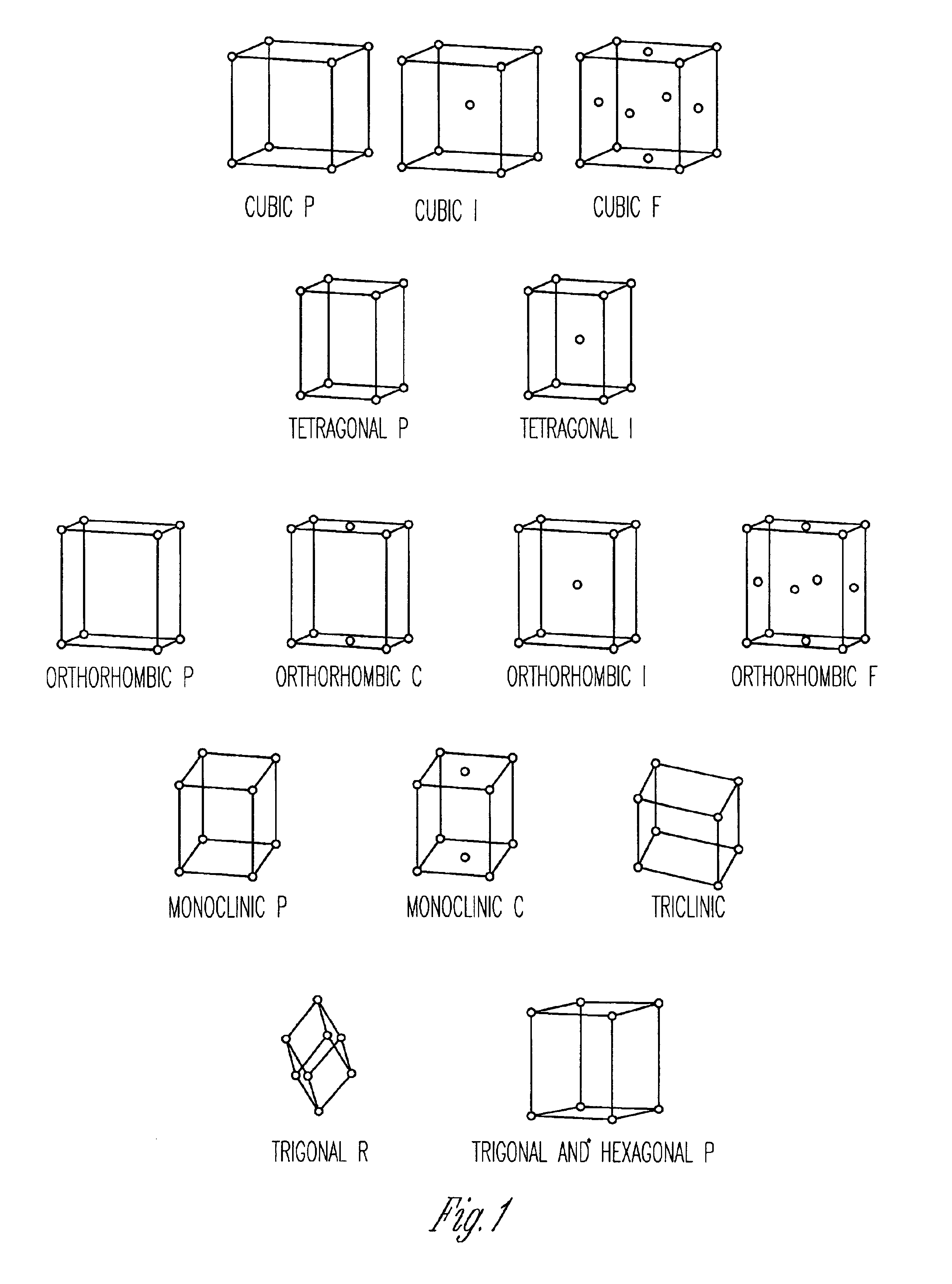
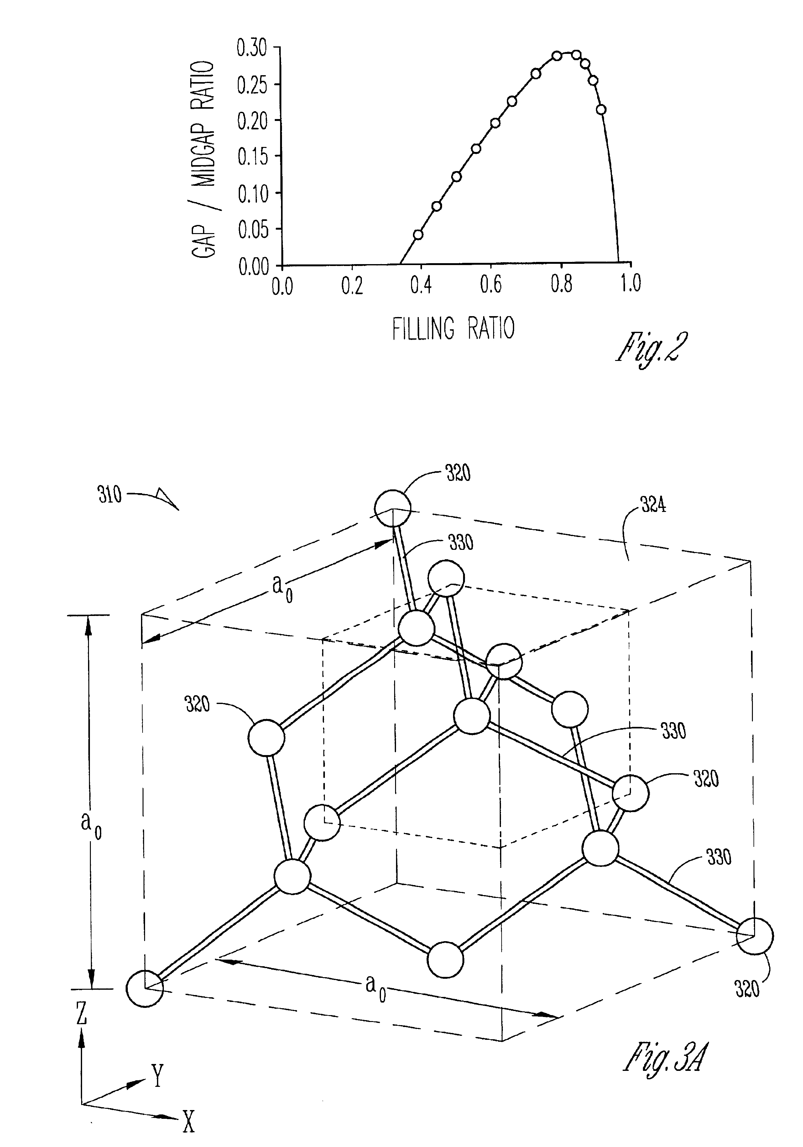

Image

  • Three-dimensional photonic crystal waveguide structure and method
  • Three-dimensional photonic crystal waveguide structure and method
  • Three-dimensional photonic crystal waveguide structure and method

Examples


Embodiment Construction

[0035]In the following detailed description of the embodiments of the invention, reference is made to the accompanying drawings that form a part hereof, and in which is shown by way of illustration specific embodiments in which the invention may be practiced. These embodiments are described in sufficient detail to enable those skilled in the art to practice the invention, and it is to be understood that other embodiments may be utilized and that changes may be made without departing from the scope of the present invention. The following detailed description is, therefore, not to be taken in a limiting sense, and the scope of the present invention is defined only by the appended claims.

[0036]The term “substrate” as used in the following description includes any material, structure or combination of material / structure for which its optical, electronic, and acoustic properties, among others, can be modified by the formation or rearrangement of photonic energy bands in such material, st...


PUM

PropertyMeasurementUnit
diameteraaaaaaaaaa
free space wavelengthaaaaaaaaaa

Abstract

A waveguide structure formed with a three-dimensional (3D) photonic crystal is disclosed. The 3D photonic crystal comprises a periodic array of voids formed in a solid substrate. The voids are arranged to create a complete photonic bandgap. The voids may be formed using a technique called “surface transformation,” which involves forming holes in the substrate surface, and annealing the substrate to initiate migration of the substrate near the surface to form voids in the substrate. A channel capable of transmitting radiation corresponding to the complete bandgap is formed in the 3D photonic crystal, thus forming the waveguide. The waveguide may be formed by interfacing two 3D photonic crystal regions, with at least one of the regions having a channel formed therein. The bandgap wavelength can be chosen by arranging the periodic array of voids to have a lattice constant a fraction of the bandgap wavelength.

Description

CROSS-REFERENCE TO RELATED APPLICATIONS[0001]This patent application is related to U.S. patent application Ser. No. 09 / 861,770 filed on May 22, 2001, and entitled “Method of forming three-dimensional photonic band structures in solid materials,” , now issued as U.S. Pat. No. 6,582,512, which is incorporated herein by reference. This patent application is also related to U.S. patent application Ser. No. 10 / 053,003, filed on Jan. 17, 2002, and entitled “Three-dimensional complete bandgap photonic crystal formed by crystal modification,” which is incorporated herein by reference.FIELD OF THE INVENTION[0002]The present invention pertains to waveguides, and in particular to waveguide structures and methods employing photonic crystals.BACKGROUND OF THE INVENTION[0003]The wave nature of electrons and the periodic lattice of atoms give rise to allowed energy bands and forbidden energy gaps for electrons in a solid. The forbidden gaps arise from the destructive interference of electrons for ...

Claims


Application Information

Patent Timeline
Patent Type & Authority Patents(United States)
IPC IPC(8): G02B6/122G02B6/12C30B33/00G02B6/13H01L21/20H01L29/04H01L29/06H01S5/10
CPCB82Y20/00C30B33/00G02B6/1225G02B6/13H01L29/04H01L29/06C30B29/60G02B2006/12078H01S5/105H01S5/11
Inventor FORBES, LEONARDGEUSIC, JOSEPH E.
Owner MICRON TECH INC
Why Eureka
Eureka Blog
Learn More