Methods and apparatus for subjecting an element to an electrical field
- Summary
- Abstract
- Description
- Claims
- Application Information
AI Technical Summary
Benefits of technology
Problems solved by technology
Method used
Image
Examples
Embodiment Construction
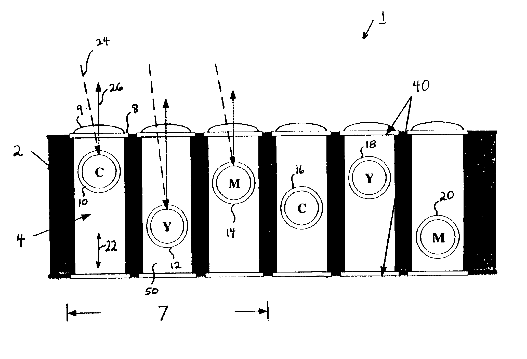
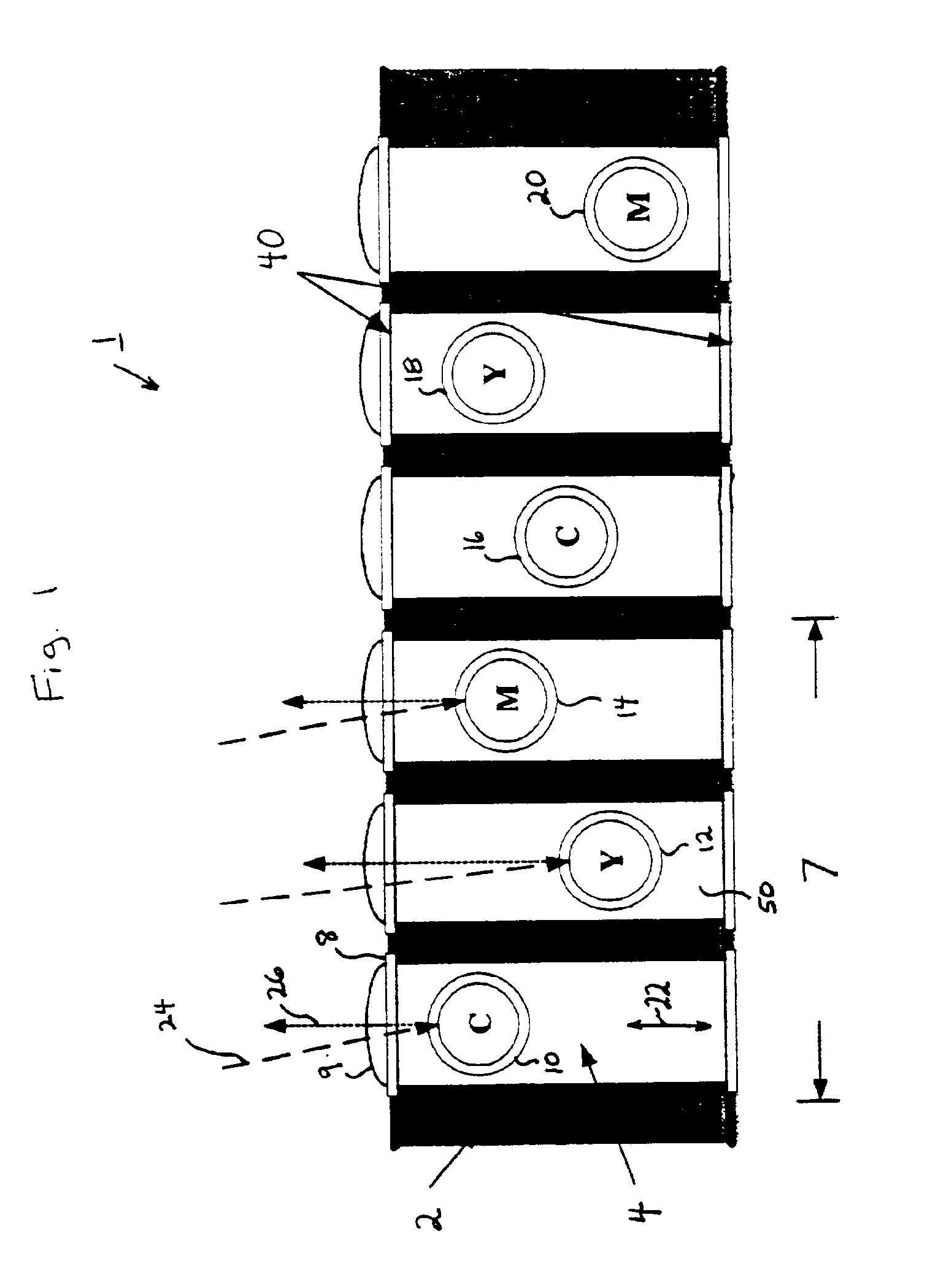
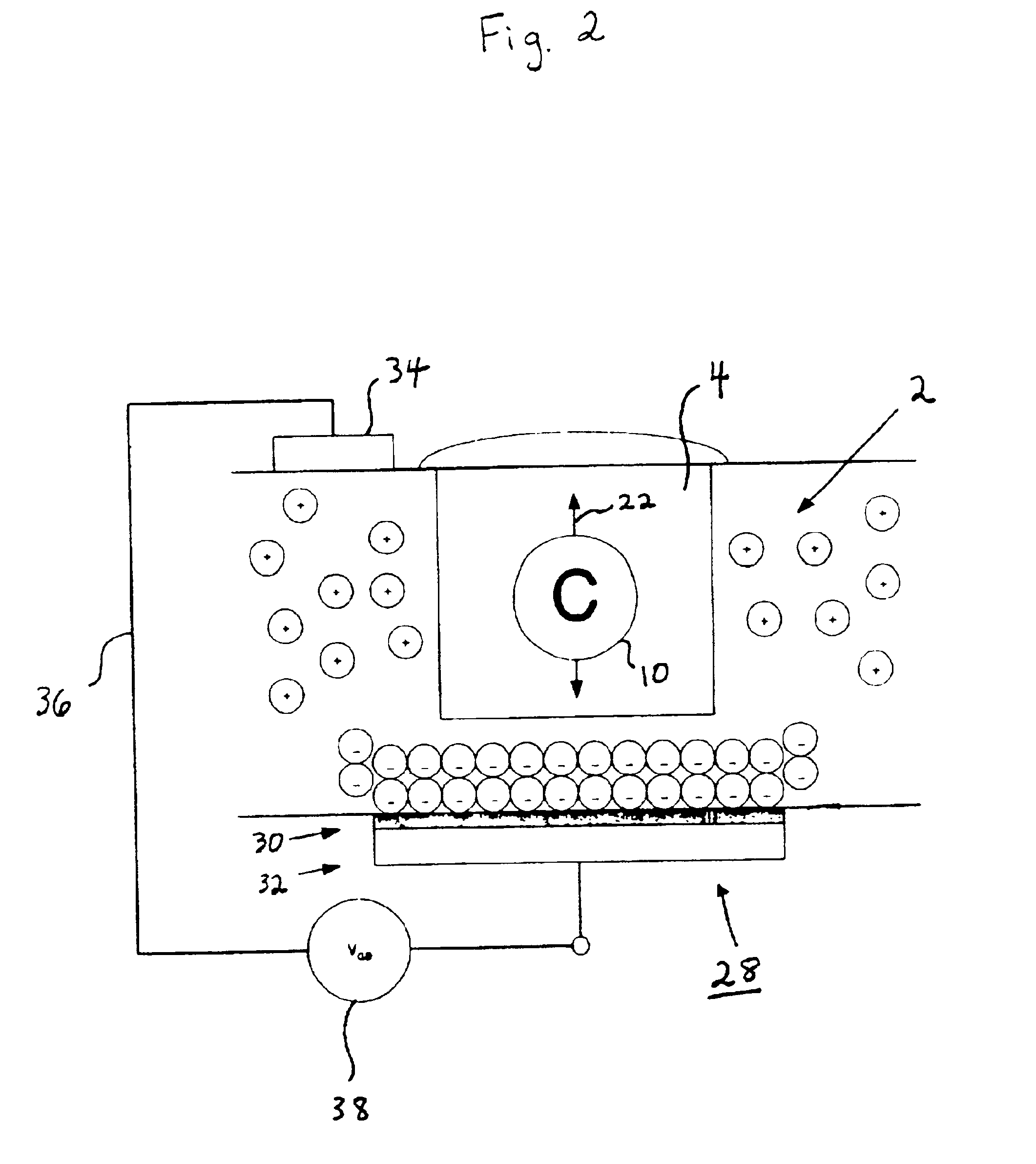
FIG. 1 is a schematic diagram that shows a display in accordance with an embodiment of the invention. The display 1 includes a carrier body 2 that defines multiple channels 4. The carrier body 2 can be made of a variety of materials, such as, for example, silicon, plastic, organic biomaterials and ceramic.
A bottom cover 6 extends across a bottom end of each of the channels 4. A top cover 8 extends across a top end of each of the channels 4. The bottom and top covers 6, 8 can close off the channels 4 so as to define a sealed area therein. Each of the top and bottom covers 6, 8 can be defined by a single sheet, or alternatively can include multiple separate elements, each element covering a single channel 4.
A lens 9 can be provided on top of each of the top covers 8 in order to enhance optical characteristics. The lens 9 can be made of a variety of materials, such as transparent plastic. The lens 9 can be defined by a single sheet, or alternatively can include multiple separate elemen...
PUM
 Abstract
Description
Claims
Application Information
 - R&D
- Intellectual Property
- Life Sciences
- Materials
- Tech Scout
- Unparalleled Data Quality
- Higher Quality Content
- 60% Fewer Hallucinations
Browse by: Latest US Patents, China's latest patents, Technical Efficacy Thesaurus, Application Domain, Technology Topic, Popular Technical Reports.
© 2025 PatSnap. All rights reserved.Legal|Privacy policy|Modern Slavery Act Transparency Statement|Sitemap|About US| Contact US: help@patsnap.com


