
Producing method of the liquid crystal display panel

Inactive Publication Date: 2005-03-29
NEC LCD TECH CORP
View PDF4 Cites 7 Cited by
  • Summary
  • Abstract
  • Description
  • Claims
  • Application Information

AI Technical Summary

Benefits of technology

Therefore, an object of the present invention is to provide a producing method of a liquid crystal display panel which makes the production processes easy and efficient.
Still another object of the present invention is to provide a producing method of a liquid crystal display panel which can prevent from damaging wirings of a substrate, generating stress in sealing materials and generating strain and distortion between substrates.
In the producing method of the present invention, a plurality of cutting grooves are formed between at least two each of device portions in the device substrate such that dividing the device substrate in the step (e) is easier.

Problems solved by technology

So, in this process, there are possibilities that the wirings of the TFT device substrate is damaged, the sealing materials receive the stress which causes damages, and strain or deviation occurs between substrates which also causes damages.
However, in the places of the second cutting, there are still possibilities that the sealing materials receive the stress which causes damages, and strain or deviation occurs between substrates which also causes damages.
That is, when using two materials of which linear expansion coefficients are largely different from each other, the possibility to start the destruction of the seal materials becomes high.

Method used


Image

  • Producing method of the liquid crystal display panel
  • Producing method of the liquid crystal display panel
  • Producing method of the liquid crystal display panel

Examples


Embodiment Construction

An embodiment of the producing method of the liquid crystal display panel of the present invention will be described below with reference to the attached drawings.

Here, a finished product is called as a liquid crystal display panel (device) and a single part before setting a deflection plate is called a cell.

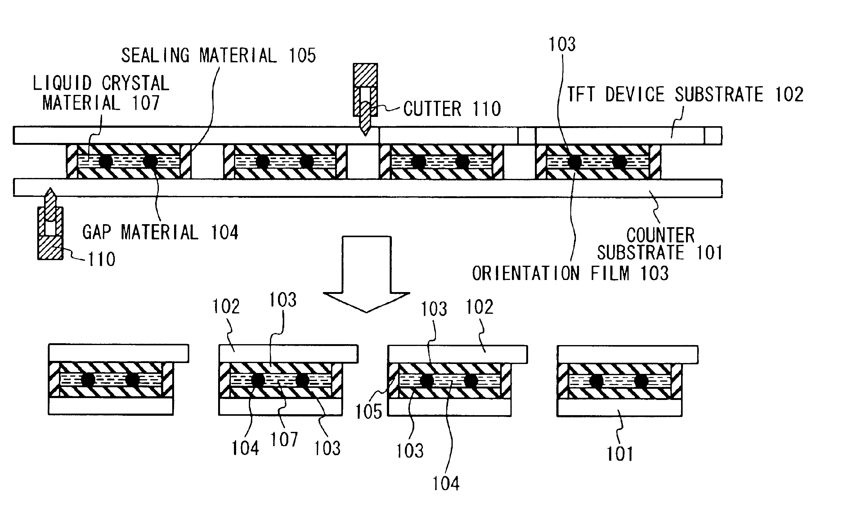
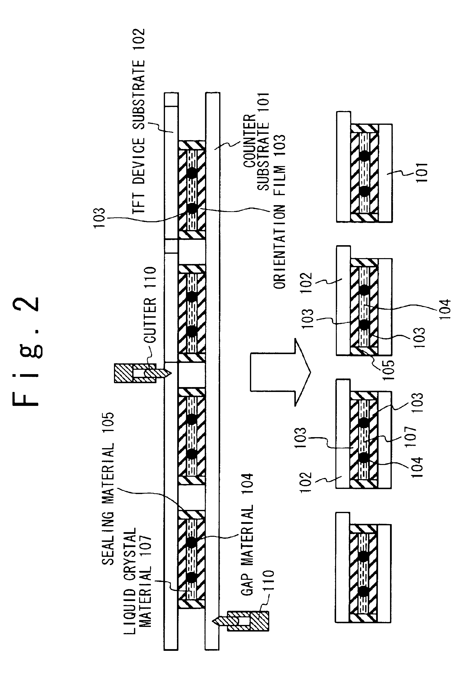
In the present invention, at least one of a TFT device substrate and a counter substrate of a liquid crystal display panel is formed from plastic film materials. In this case, the substrate becomes lightweight and moreover thin. Also, the counter substrate is cut down to a plurality of single parts for the cells. Next, a liquid crystal material is dropped onto the counter substrate by a drop filling (ODF:One Drop Fill) method. Then, the TFT device substrate after sealing up is cut down to a plurality of single parts for the cells. By this method, it can be easy and efficient to produce the cells in the high yield.

FIG. 3 is a view showing a flow chart of the embodiment of the pro...


PUM


Abstract

A producing method of a liquid crystal display panel includes steps (a) to (e). The Step (a) is fixing a counter substrate on a fixing table, wherein the counter substrate includes a plurality of counter portions each of which includes a plurality of counter electrodes. The Step (b) is dividing the counter substrate into the plurality of counter portions. The Step (c) is putting a liquid crystal material on the each of plurality of counter portions. The Step (d) is attaching a device substrate and the counter substrate together, wherein the device substrate includes a plurality of device portions each of which includes a plurality of switching devices. The Step (e) is dividing the device substrate into the plurality of device portions. The each of plurality of device portions is attached to a corresponding one of the each of plurality of counter portions.

Description

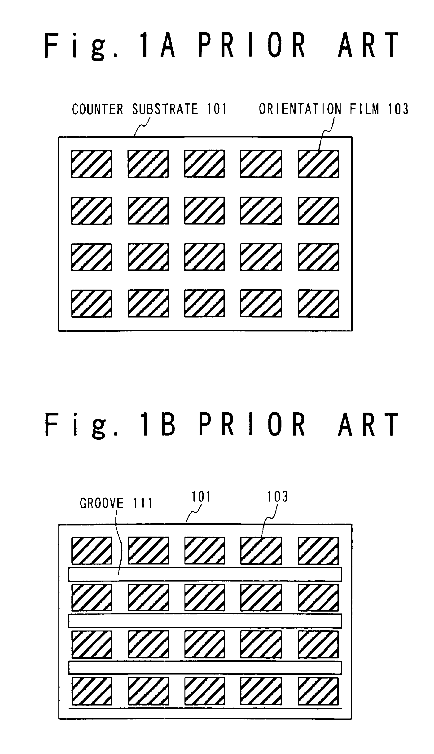
BACKGROUND OF THE INVENTION1. Field of the InventionThe present invention relates to a producing method of the liquid crystal display panel.2. Description of the Related ArtHere, a finished product is called as a liquid crystal display device and a single part before setting a deflection plate is called a cell.Conventionally, a liquid crystal display panel is produced by a following method: attaching a TFT device substrate to a counter substrate, dropping the liquid crystal material into a gap between these substrates, sealing a peripheral end of the gap with a sealing material, and then, cutting an assembly of the TFT device substrate and the counter substrate to obtain cells.The conventional technique forming the cell will be described with reference to the Japanese Laid Open Patent Application (JP-A-Heisei 5-107517).FIGS. 1A and 1B are plan views showing the conventional technique of the counter plates before and after being cut. As shown in FIG. 1A, the counter substrate 101 is ...

Claims


Application Information

Patent Timeline
IPC IPC(8): G02F1/13G02F1/1333B26F1/40G02F1/1341G02F1/1368
CPCG02F1/133351G02F2001/13415G02F2001/133354G02F1/133354G02F1/13415G02F1/13
Inventor NOIRI, YOSHIKAZUHORIUCHI, TOSHIHIROMUKAI, TOSHIAKIUEEBISU, SHINJIYOSHIZOE, HIDEFUMI
Owner NEC LCD TECH CORP
Learn More