Enhanced fuse configurations for low-voltage flash memories

a low-voltage flash memory and fuse configuration technology, applied in the field of fuse configurations, can solve the problems of inability to meet the memory device of today, memory cell may become defective, memory device inoperable or unreliable,

Inactive Publication Date: 2005-01-25
MICRON TECH INC
View PDF21 Cites 13 Cited by
  • Summary
  • Abstract
  • Description
  • Claims
  • Application Information

AI Technical Summary

Benefits of technology

In another illustrative embodiment, a method is discussed for enhancing a fuse circuit in a low-voltage integrated circuit (IC). The method includes presenting by an input stage an inverted enabling signal, boosting by a boosting stage the inverted enabling si

Problems solved by technology

A memory cell may become defective because of imperfect manufacturing practices or degradation over time.
Such defects render the memory device inoperative or unreliable.
Previous generations of fuse circuits are incompatible with the memory devices of today, which use voltage supplies as low as 1.65 volts.
Such integration causes inflexibility that is undesirable.

Method used


Image

  • Enhanced fuse configurations for low-voltage flash memories
  • Enhanced fuse configurations for low-voltage flash memories
  • Enhanced fuse configurations for low-voltage flash memories

Examples


Embodiment Construction

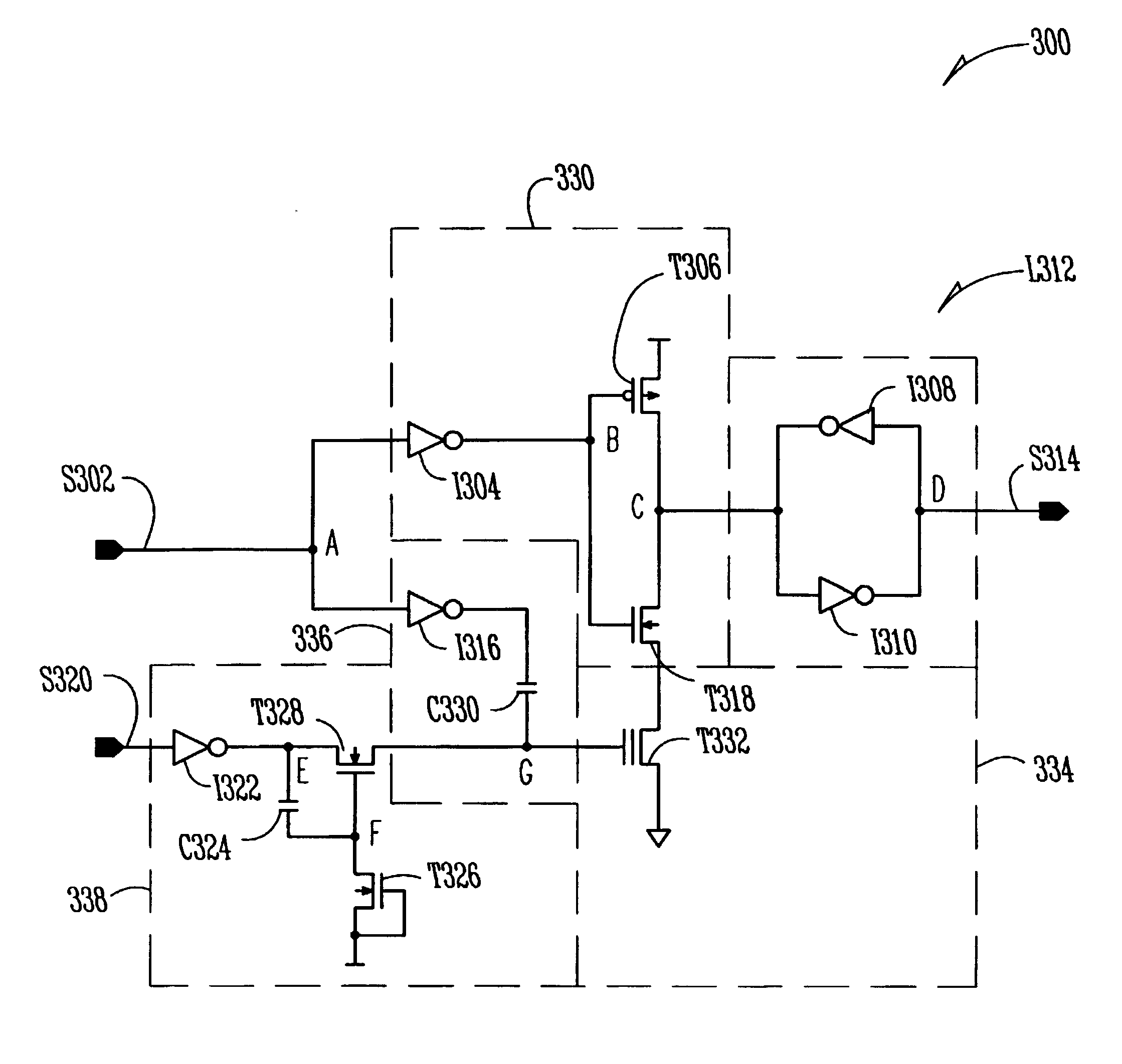
In the following detailed description of the invention, reference is made to the accompanying drawings that form a part hereof, and in which is shown, by way of illustration, specific embodiments in which the invention may be practiced. In the drawings, like numerals describe substantially similar components throughout the several views. These embodiments are described in sufficient detail to enable those skilled in the art to practice the invention. Other embodiments may be utilized and structural, logical, and electrical changes may be made without departing from the scope of the present invention.

The transistors described herein include transistors from bipolar-junction technology (BJT), field-effect technology (FET), or complementary metal-oxide-semiconductor (CMOS) technology. A metal-oxide-semiconductor (MOS) transistor includes a gate, a first node (drain) and a second node (source). Since a MOS is typically a symmetrical device, the true designation of “source” and “drain” i...


PUM


Abstract

An enhanced fuse circuit is discussed that advances redundancy techniques in integrated circuits. The enhanced fuse circuit uses a single nonvolatile fuse and a latch that is coupled at a desired time. One embodiment of the invention discusses a fuse circuit that includes a volatile latch and a nonvolatile fuse. The nonvolatile fuse adapts to operate with a voltage supply greater than about 1.65 volts. The voltage supply is boosted at a desired time to a predetermined level and for a predetermined duration so that the nonvolatile fuse transfers its data to the volatile latch.

Description

TECHNICAL FIELDThe present invention relates generally to semiconductor integrated circuits. More particularly, it pertains to fuse configurations that are used in redundancy circuits in low-voltage flash memory devices.BACKGROUNDMemory devices are integrated circuits in which information may be stored and from which information may be extracted when desired. Each memory device is built from a plurality of memory cells. Each memory cell memorizes a bit of data. Although a bit of data seems insignificant, it may determine whether the stored information is correct, such as an amount in a bank account.A memory cell may become defective because of imperfect manufacturing practices or degradation over time. Such defects render the memory device inoperative or unreliable. Instead of ridding memory devices with defective memory cells, the semiconductor industry turns to various techniques to salvage these memory devices.One technique employs redundancy circuits. Redundancy circuits include...

Claims


Application Information

Patent Timeline
IPC IPC(8): G11C29/00G11C29/04G11C16/06H01L21/82
CPCG11C29/70G11C29/00
Inventor SANTIN, GIOVANNI
Owner MICRON TECH INC
Why Eureka
Try Eureka