
Dynamically re-configurable CMOS imagers for an active vision system

a dynamic reconfigurable, imager technology, applied in the field of active vision system, can solve the problems of high imaging quality, high complexity of the active vision system, and inability to be easily handled by the conventional imaging system

Inactive Publication Date: 2005-01-04
CALIFORNIA INST OF TECH
View PDF9 Cites 140 Cited by
  • Summary
  • Abstract
  • Description
  • Claims
  • Application Information

AI Technical Summary

Problems solved by technology

However, an active vision system may involve high degree of complexity because it concurrently carries out a number of diverse visual tasks.
These visual tasks may include search, detection, recognition, and unresolved multi-target tracking, which may not be easily handled by conventional imaging systems.
Furthermore, many active vision applications involve scenes with low contrast, requiring high imaging quality.
The serial nature of the data output from the imager and the nature of sampling of the scene impose unacceptable limitations on power, speed, and volume of the imaging system.
Moreover, data processing complexity grows as O(n), where n is the number of pixels output to the off-chip processor.
For such imaging systems, the serial nature of pixel access and the enormity of the data volume impose the greatest bottleneck in coupling an imager to an off-chip processor.
Furthermore, most of the power dissipation of an imager is concentrated in the output stage that requires high-speed drive into a large load.
However, since the acuity variation is hard-wired, the vision system requires mechanical pointing.
Moreover, the size, power consumption, and the slow response times of mechanical pointing systems preclude an efficient realization of a low-power, miniature, real-time active vision system.

Method used


Image

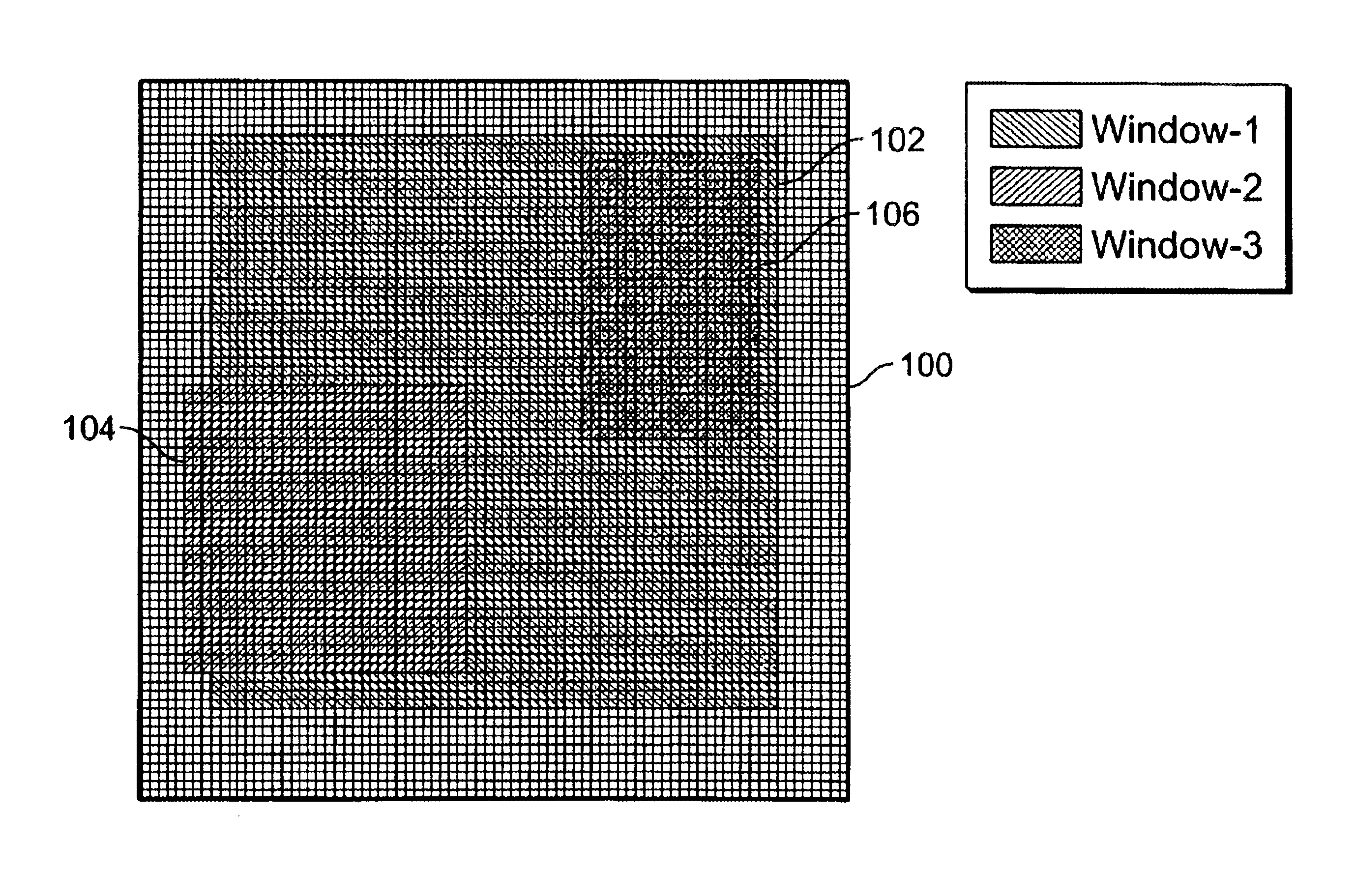
  • Dynamically re-configurable CMOS imagers for an active vision system
  • Dynamically re-configurable CMOS imagers for an active vision system
  • Dynamically re-configurable CMOS imagers for an active vision system

Examples


Embodiment Construction

Introduction

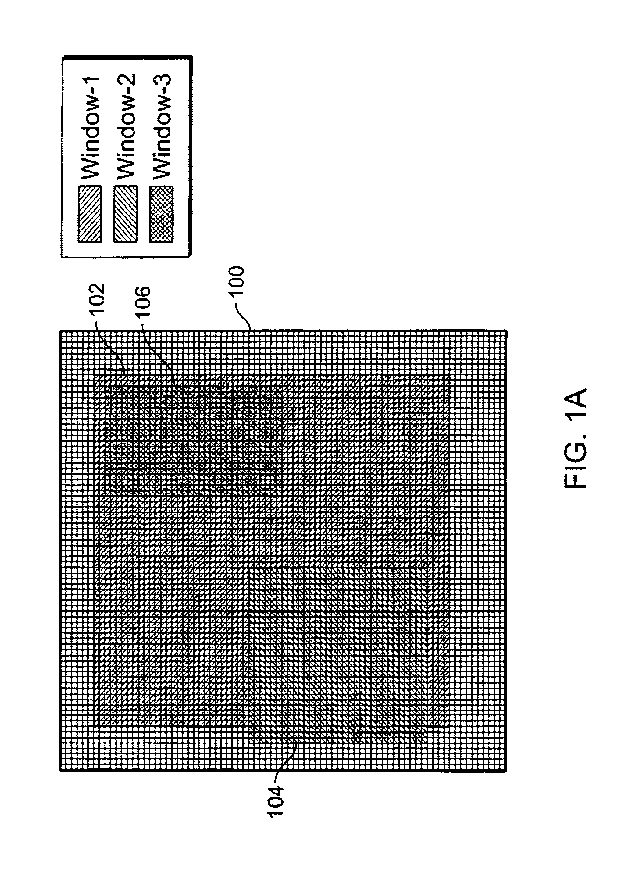
The inventors recognized that existing biological vision imagers, such as foveal vision imagers with on-chip foveated structures, suffer from at least three difficulties. First, the multi-resolution lattice is hard-wired, and may not be programmed by the user. Secondly, the high-resolution window is located near the center, effectively restricting the field of view (FOV) and requiring accurate mechanical control of an imager head. Thirdly, the lattice is configured in a log-polar topology that may be sensitive to alignment errors, and may not be compatible with readily available programs.

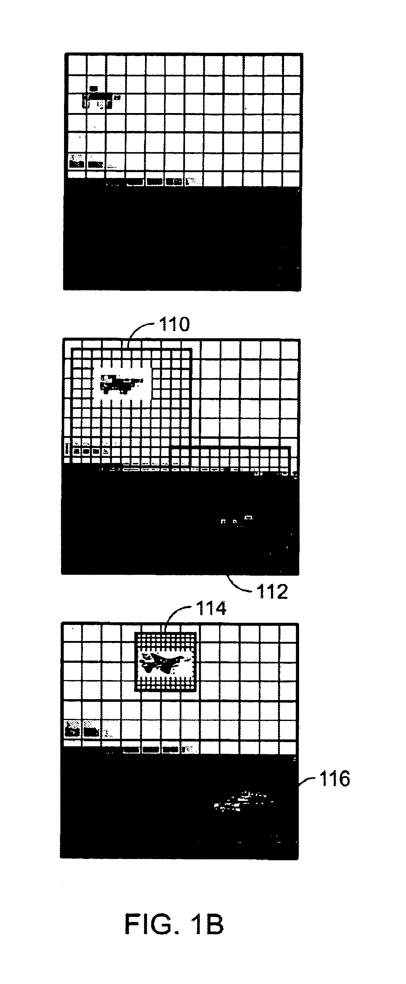
Therefore, the present disclosure provides methods and systems to substantially reduce the bottleneck presented by the serial nature of pixel access, to reduce power, and to substantially reduce the use of mechanical pointing systems. To achieve these characteristics, the present system of the active vision chip provides output only from user-selected multiple regions of interest (ROI). ...


PUM


Abstract

A vision system is disclosed. The system includes a pixel array, at least one multi-resolution window operation circuit, and a pixel averaging circuit. The pixel array has an array of pixels configured to receive light signals from an image having at least one tracking target. The multi-resolution window operation circuits are configured to process the image. Each of the multi-resolution window operation circuits processes each tracking target within a particular multi-resolution window. The pixel averaging circuit is configured to sample and average pixels within the particular multi-resolution window.

Description

BACKGROUNDThe present disclosure generally relates to an active vision system, and more specifically, to dynamically re-configurable CMOS imagers used in such a system.Active vision systems are of interest in realizing autonomous systems. These systems range from commercial and industrial applications to surveillance and military applications. The commercial and industrial applications may involve mobile robots, unmanned vehicles including self-navigating cars and search-and rescue vehicles, automatic assembly and product inspection systems. The surveillance and military applications may involve smart weapons and missile defense systems. Active vision systems are also of interest in space applications involving vehicles for space transportation that require autonomous docking and rendezvous with space stations, robotic exploration of planets, and autonomous rovers. However, an active vision system may involve high degree of complexity because it concurrently carries out a number of ...

Claims


Application Information

Patent Timeline
IPC IPC(8): H04N3/15
CPCH03F3/082H04N3/1562H03F2200/375H04N25/445H04N25/443H04N25/46
Inventor YANG, GUANGPAIN, BEDABRATA
Owner CALIFORNIA INST OF TECH
Learn More