
Epitaxial oxide films via nitride conversion

Inactive Publication Date: 2003-11-11
APPL THIN FILMS INC
View PDF8 Cites 17 Cited by
  • Summary
  • Abstract
  • Description
  • Claims
  • Application Information

AI Technical Summary

Benefits of technology

It is yet another object of the invention to provide a method for obtaining good quality epitaxial oxides without premature substrate oxidation.
Multiple layers of different nitrides can be deposited with high rates and converted to oxide sequentially, if such a configuration is required for a specific application--depending on structural, electro-magmentic / optical, mechanical or thermal properties of oxide and nitride. For example, a thin ZrN layer can be deposited on a substrate to improve the epitaxial quality / in-plane orientation of a YZN film deposited thereon. See, for instance, Example 15. As a further example, a thin epitaxial TiN layer can be first deposited on Ni substrate, rather than YZN, because it has smaller lattice mismatch with Ni (19%) than YZN (31%) and allows for more straightforward growth process. A thick YZN layer can then be deposited on TiN-coated Ni or other metal or metal alloy substrates, relatively easily due to the smaller mismatch between YZN and TiN (.about.10%). Subsequent oxidative conversion produces an epitaxial TiO.sub.x / YSZ composite on Ni. Epitaxial nitrides can also be deposited on biaxially textured metal / alloy substrates at high rates even when a large lattice mismatch between nitride and substrate is present.

Problems solved by technology

There are numerous problems related to the prior art as pertains to the use and deposition of oxide layers on metal / alloy substrates.

Method used


Image

  • Epitaxial oxide films via nitride conversion
  • Epitaxial oxide films via nitride conversion
  • Epitaxial oxide films via nitride conversion

Examples


example 1

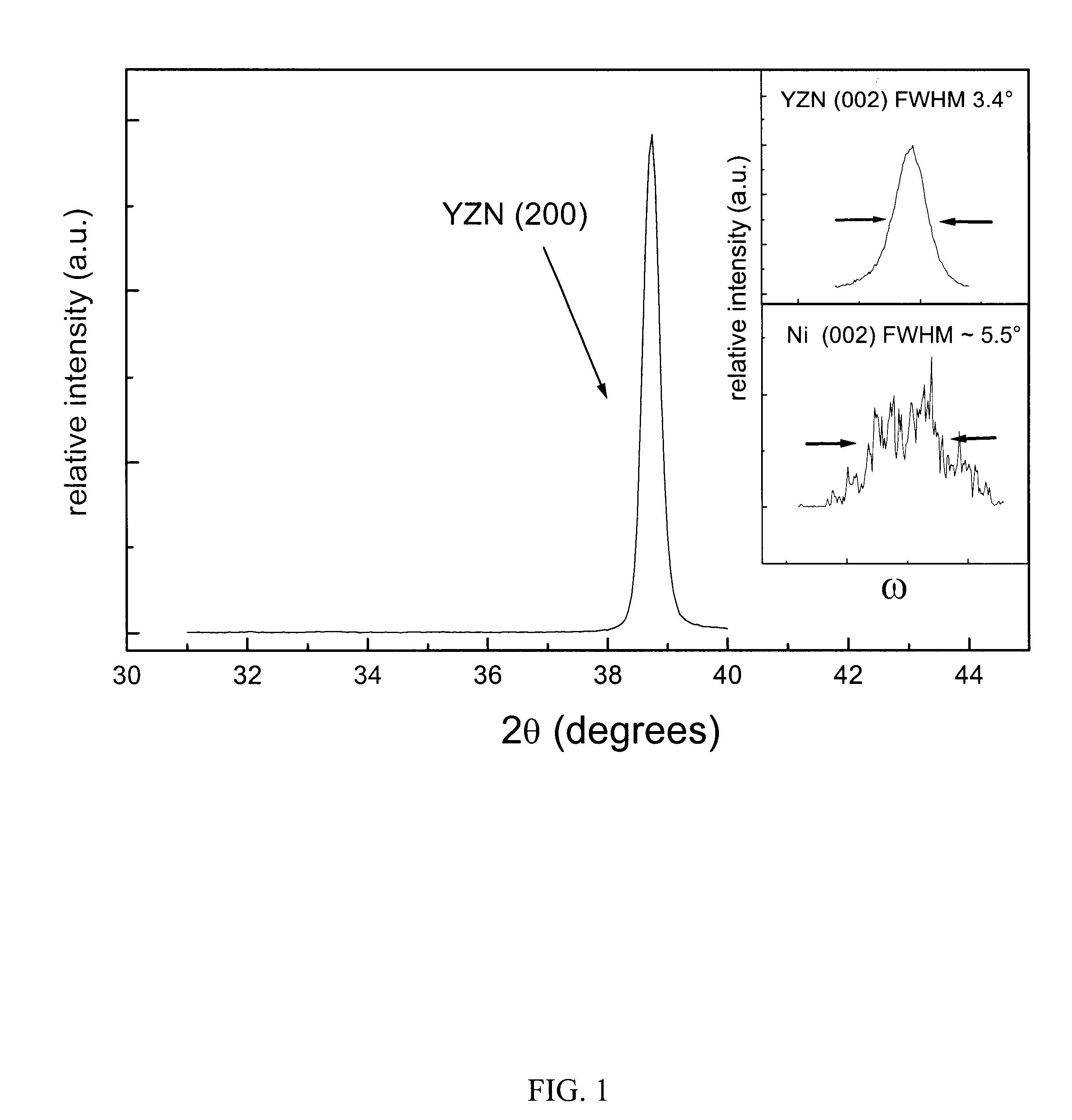
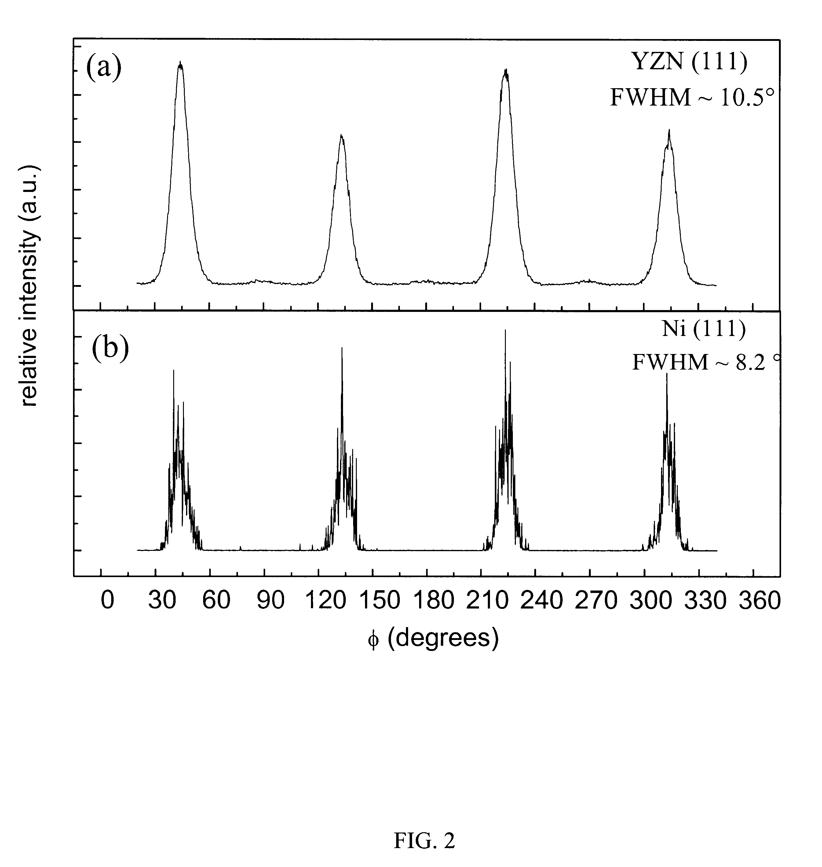
Magnetron sputtered (Zr.sub.0.8 Y.sub.0.2)N (YZN) films were grown on biaxially textured Ni substrate, using a two temperature technique. Initially growth was done at 500.degree. C. until the YZN thickness reached .about.30 nm. Then the growth temperature was raised to 700.degree. C. and remained the same for rest of the deposition. Total film thickness was .about.200 nm and a deposition rate of 0.12 nm / sec. The films showed good in-plane and out-of-plane alignment. FIG. 1 shows a XRD .theta.-2.theta. scan, and FIG. 2 shows the (111) pole figure. The existence of only four peaks demonstrates a single epitaxial orientation. The location of the peaks in the (111) pole figure is consistent with a cube-on-cube epitaxial relationship. The YZN (111) phi scan showed a full-width-half-maximum (FWHM) obtained by fitting a Gaussian curve to the data to be 10.5.degree.. The FWHM is only slightly better than that of the underlying Ni with a FWHM of .about.8.2.degree.. The rocking curves FWHM (t...

example 2

Magnetron sputtered (Zr.sub.0.8 Y.sub.0.2)N (YZN) films were grown at a substrate temperature of .about.550.degree. C. on biaxially textured nickel substrates at a deposition rate of 0.12 nm / sec. The films had a thickness of 50 nm. The films showed in-plane and out-of-plane alignment. FIG. 3 shows a XRD .theta.-2.theta. scan, shows intense (200) peak. The presence of a (111) peak indicates that this sample has substantial out of plane texture in (200) direction but is not epitaxial. FIG. 4 shows the (111) phi-scan from same sample. The location of the peaks in the (111) phi peaks is consistent with a cube-on-cube epitaxial relationship. The YZN (111) phi scan showed a full-width-half-maximum (FWHM) obtained by fitting a Gaussian curve to the data to be 10.9.degree., indicating the grains that aligned to (200) orientation in out-of-plane direction also has some in-plane textures. The rocking curve FWHM (the out-of-plane texture) of the YZN layer was found to be 5.8.degree. in rolling...

example 3

Y.sub.0.5 Z.sub.0.5 N films have been grown on single crystal MgO using reactive magnetron sputtering in order to study the solid solution range in the YN--ZrN system. Growth was carried out in Ar--N.sub.2 mixtures. Typical growth temperatures ranged from 400.degree. C. to 800.degree. C. and typical growth rates were 0.2 nm / sec. For deposition of Y.sub.0.5 Z.sub.0.5 N, 99.95% pure Y and Zr targets were used. FIG. 5 shows .theta.-2.theta. x-ray diffraction (XRD) scan of a nominal Y.sub.0.5 Z.sub.0.5 N film grown on MgO. The thickness of film was 50 nm. The pattern clearly shows presence of both YN and ZrN phases suggesting a phase miscibility gap existing in the YN--ZrN pseudo-binary system.


PUM

PropertyMeasurementUnit
thickaaaaaaaaaa
radiiaaaaaaaaaa
partial pressureaaaaaaaaaa

Abstract

The present invention relates to oxides on suitable substrates, as converted from nitride precursors.

Description

The present invention relates generally to epitaxial metal oxide films and, more particularly, to those films and related composite structures as can be prepared by oxidizing a previously deposited nitride layer.Recent emergence of high-temperature superconducting (HTS) thick-film tape technology is expected to meet the cost, size and performance requirements of superconducting components needed for advanced power applications for the defense and commercial sectors. One of the major potential HTS applications is in the electric power industry.The YBa.sub.2 Cu.sub.3 O.sub.7 and related ceramic materials (YBCO) have appropriate intrinsic properties in the liquid nitrogen temperature range. However, their properties are drastically affected by grain boundary misorientations. In order to provide high temperature and field applications, it is imperative that a biaxially textured, polycrystalline YBCO tape, or related article, be developed which contains few high angle grain boundaries.A ...

Claims


Application Information

Patent Timeline
Patent Type & Authority Patents(United States)
IPC IPC(8): C30B33/00C23C8/02C30B23/02H01L39/24C30B29/22C23C14/06C23C14/08H01L21/318
CPCC23C8/02C30B23/02C30B29/38C30B33/005C30B29/225H01L39/2461C30B29/22H10N60/0632B32B15/04
Inventor SAMBASIVAN, SANKARBARNETT, SCOTT A.KIM, ILWONRECHNER, JOHN
Owner APPL THIN FILMS INC
Learn More