
Sequential burst mode activation circuit

a burst mode and activation circuit technology, applied in the direction of electric variable regulation, process and machine control, instruments, etc., can solve the problems of current ripple, inverter performance retardation, and discharging becoming unstabl

Inactive Publication Date: 2002-12-31
O2 MICRO INT LTD
View PDF97 Cites 148 Cited by
  • Summary
  • Abstract
  • Description
  • Claims
  • Application Information

AI Technical Summary

Benefits of technology

The solution effectively eliminates flicker and noise in multiple lamp configurations by ensuring that each load receives a phase-shifted burst signal, allowing for a larger dimming ratio and improved consistency in light intensity variation without current ripples.

Problems solved by technology

As the fluorescent tube emits light using discharging energy, when the application voltage to the fluorescent tube is too low, the discharging becomes unstable.
If multiple CCFLs (cold cathode fluorescent lamps) were utilized, synchronization of all lamps with one light source would result in current ripples; these current ripples retard inverter performance and cause flicker.
The instant power delivered from the power supply causes the supply voltage to drop due to its limited dynamic response.
Therefore, the use of PWM signals, i.e. "burst-mode" dimming, is not, by itself, effective in providing a solution to flicker / noise in multiple lamp configurations.
A drawback of this technique is that, when the lamps turn off in each burst mode cycle, the power supply line, which has an intrinsic inductance, continues to carry current which charges the capacitor, yielding an increase in output voltage.
Prior art teachings with the activation with multiple loads, where the loads are not fluorescent lamps, do not address the flicker or noise problem presented by the activation of multiple lamps.

Method used


Image

  • Sequential burst mode activation circuit
  • Sequential burst mode activation circuit
  • Sequential burst mode activation circuit

Examples


Embodiment Construction

The following description will reference a burst mode regulating circuit for a plurality of cold cathode fluorescent lamps (CCFLs). CCFLs are arranged, for example, in large panels for displays. Typically, large CCFL panels each utilize a minimum of 6 lamps, and the present invention will describe a burst mode activation circuit with 6 or more CCFls. Of course, the present invention is not to be limited by a minimum number of loads, nor is it to be limited to CCFLs or any particular type of loads.

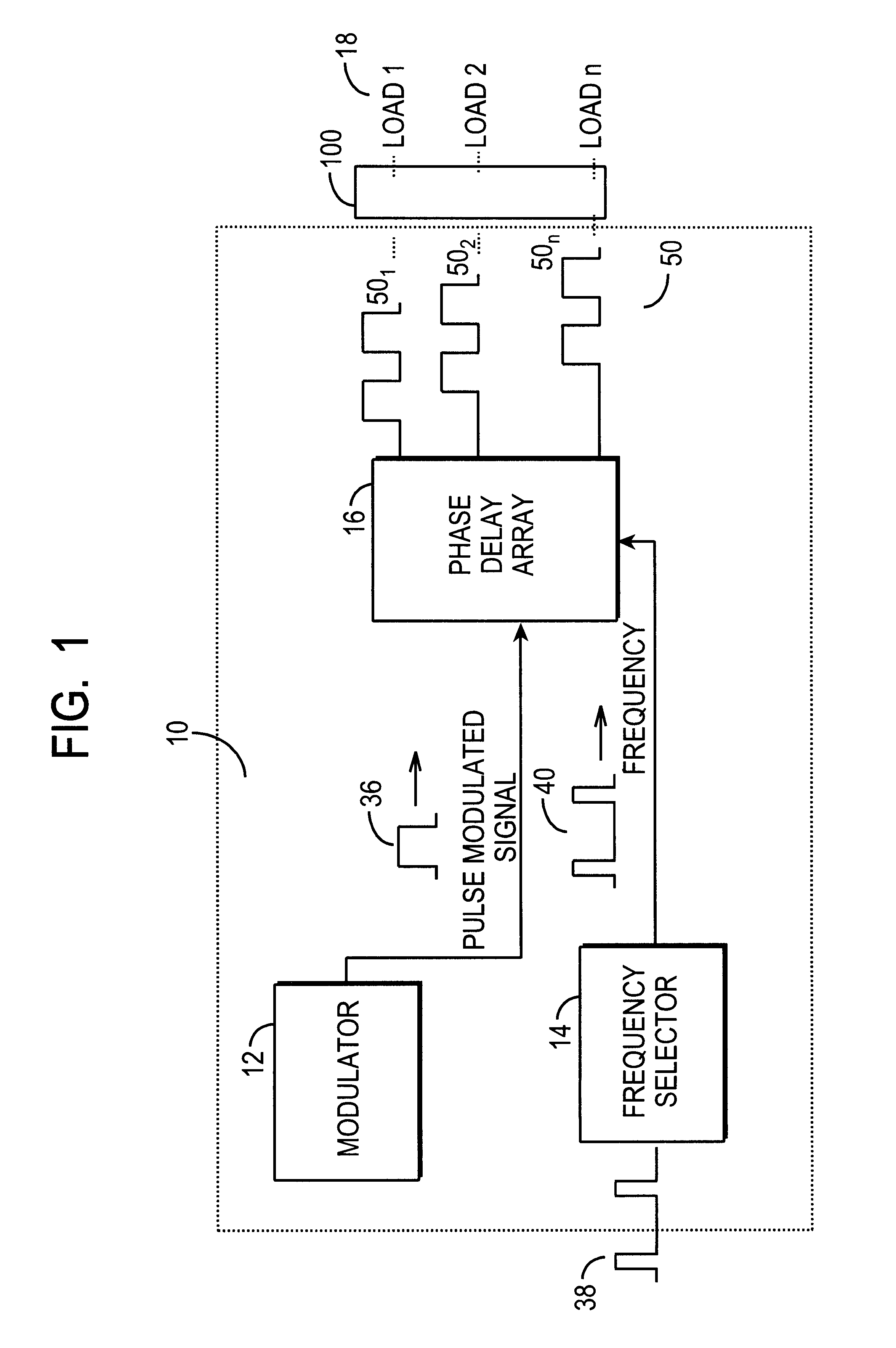
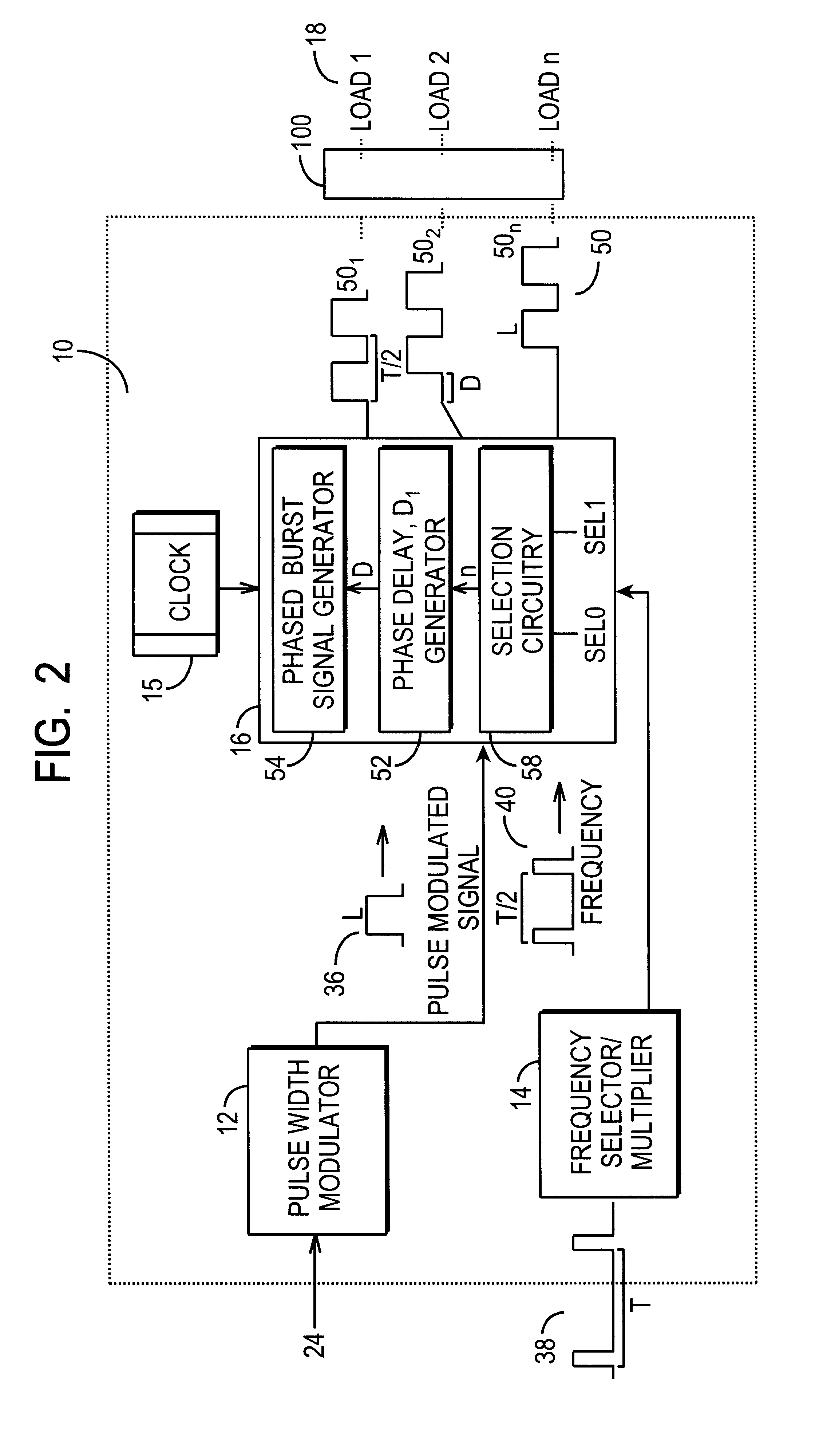
FIG. 1 is a top-level block diagram of an exemplary sequential burst mode signal generation system 10 of the present invention. As a general overview, the sequential burst mode signal generation system 10 operates to generate phase-shifted burst mode signals 50 and sends these burst mode signals to drivers 100 to provide time-delayed regulation of power to a plurality of loads 18. "Burst mode", as used herein and as is understood in the art, generally means regulation of power to a load usi...


PUM


Abstract

A sequential burst mode regulation system to deliver power to a plurality of loads. In the exemplary embodiments, the system of the present invention generates a plurality of phased pulse width modulated signals from a single pulse width modulated signal, where each of the phased signals regulates power to a respective load. Exemplary circuitry includes a PWM signal generator, and a phase delay array that receives a PWM signal and generates a plurality of phased PWM signals which are used to regulate power to respective loads. A frequency selector circuit can be provided that sets the frequency of the PWM signal using a fixed or variable frequency reference signal.

Description

1. Field of the InventionThe present invention relates to a sequential burst mode activation circuit. More particularly, the present invention provides a circuit topology for improving the consistency of performance in the activation and intensity variation of multiple loads. The present invention has general utility wherever multiple loads are employed for intensity variation. Further, the present invention has specific utility where multiple fluorescent lamps, especially multiple cold cathode fluorescent lamps (CCFLs), are employed, for example, in television and computer screens, and in backlights for LCDs (Liquid Crystal Displays).2. Description of Related ArtVarious lighting and dimming circuits and techniques for lighting or dimming lamps or varying intensities of loads are known. One method of dimming a fluorescent lamp, especially as used in a backlight of a liquid crystal display (LCD), is known as a voltage controlled dimming system. The voltage controlled dimming system i...

Claims


Application Information

Patent Timeline
Patent Type & Authority Patents(United States)
IPC IPC(8): H02M1/00H02J1/14H05B41/39H05B41/392H02M1/36
CPCH02J1/14H02M1/36H05B41/3927H02M2001/008H02M1/008H02M7/527
Inventor LIN, YUNG-LINCHANG, YU-CHENGYAO, BINGWEI
Owner O2 MICRO INT LTD
Learn More