
Complex circuit board with an electrode and air gap between dielectric and magnetic substrates

a dielectric and magnetic substrate technology, applied in the field of complex circuit boards, can solve the problems of lowering the non-reciprocity of devices, unable to miniaturize elements, and unable to increase inductance by a limited valu

Inactive Publication Date: 2002-10-29
MURATA MFG CO LTD
View PDF13 Cites 18 Cited by
  • Summary
  • Abstract
  • Description
  • Claims
  • Application Information

AI Technical Summary

Benefits of technology

In another arrangement, a substrate having electrodes on its top and bottom faces, the electrodes being connected by a through hole, may be provided between the dielectric substrate and the magnetic substrate.
As a consequence, there is no need to connect the electrode on the dielectric substrate to the electrode on the magnetic substrate, eliminating problems of reduced reliability and time-consuming manufacturing processes which such connection causes.

Problems solved by technology

However, when a dielectric substrate is provided nearby, the coupling of the resonator portion to the dielectric is strengthened, lowering the nonreciprocity of the device.
Therefore, when the capacitance element, the inductance element, and the like formed by the electrode pattern, clasped between the dielectric substrate and the magnetic substrate, are provided within a single plane, there are disadvantages that the inductance can be increased only by a limited value, the elements cannot be miniaturized, and consequently the complex circuit board cannot be miniaturized.
There is an additional disadvantage that it is not possible to precisely design the characteristics of the capacitance element, the inductance element, the resistor, the transmission lines, and the like.

Method used


Image

  • Complex circuit board with an electrode and air gap between dielectric and magnetic substrates
  • Complex circuit board with an electrode and air gap between dielectric and magnetic substrates
  • Complex circuit board with an electrode and air gap between dielectric and magnetic substrates

Examples


Embodiment Construction

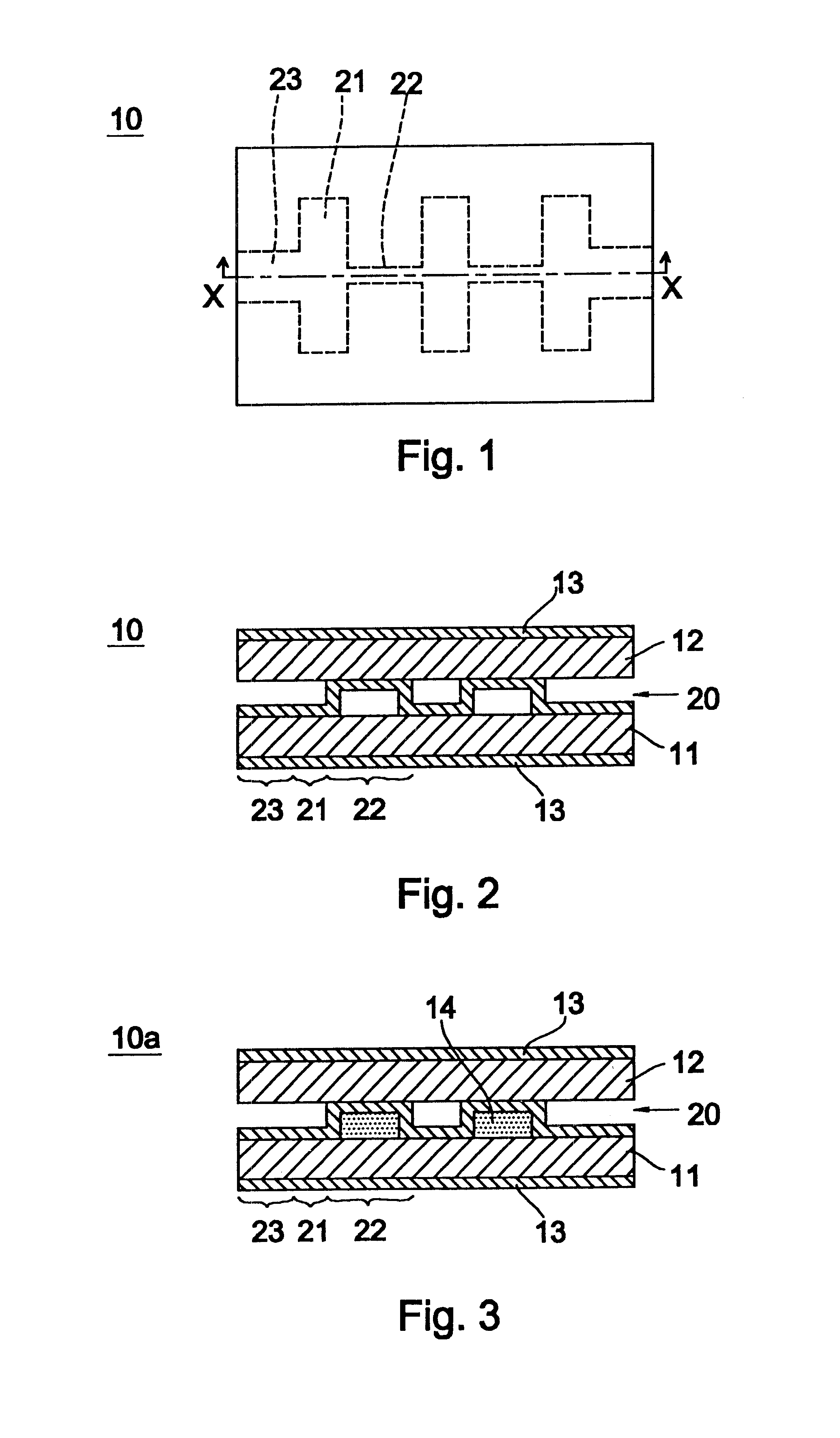
A complex circuit board according to a preferred embodiment of the present invention will be described below with reference to FIGS. 1 and 2. FIG. 1 is a plan view of a complex circuit board of the present invention, and FIG. 2 is a cross-sectional view taken along the line X--X of FIG. 1.

As shown in FIGS. 1 and 2, the complex circuit board 10 of the present invention comprises a dielectric substrate 11, a magnetic substrate 12, and an electrode pattern 20 clasped therebetween. The electrode pattern 20 comprises a capacitance element portion 21, an inductance element portion 22, a transmission line portion 23, and the like. Ground electrodes 13 are provided on outside faces of the dielectric substrate 11, comprising for instance CaTiO.sub.3, and the magnetic substrate 12, comprising ferrite. The complex circuit board 10 having the constitution shown in FIG. 1 functions here as a low-pass filter.

As shown in FIG. 2, in the complex circuit board 10 of the present invention, the capacit...


PUM


Abstract

In a complex circuit board, the positional relationships between element portions, including an electrode pattern, a dielectric substrate and a magnetic substrate, can be adjusted as desired, and the complex circuit board can be miniaturized. The complex circuit board includes a dielectric substrate and a magnetic substrate, a space being provided between the magnetic substrate and the dielectric substrate, and an electrode pattern provided between the dielectric substrate and the magnetic substrate, a capacitance element portion of the electrode pattern being provided adjacent or in contact with or spaced a predetermined distance from the dielectric substrate, and the inductance element portion of the electrode pattern being provided adjacent or in contact with or spaced a predetermined distance from the magnetic substrate.

Description

1. Field of the InventionThe present invention relates to a complex circuit board comprising an electrode clasped between a dielectric substrate and a magnetic substrate, a nonreciprocal circuit device, a resonator, a filter, a duplexer, a communications device, a circuit module, a method for manufacturing the complex circuit board, and a method for manufacturing the nonreciprocal circuit device.2. Description of the Related ArtConventionally, dielectric substrates or magnetic substrates having electrode patterns thereon, forming a capacitance element and / or an inductance element, for example, have been laminated in multiple stages to form a resonator circuit or the like. Depending on the application and desired characteristics and the like, low-profiling is sometimes required, and a conventional complex circuit board has been devised to satisfy such requirements.A conventional complex circuit board will be explained based on FIGS. 23 and 24. FIG. 23 is a plan view of a conventional...

Claims


Application Information

Patent Timeline
IPC IPC(8): H01P1/387H01P11/00H01P1/215H01P1/20H01P1/32H05K1/16H05K1/02H01P1/203H01P1/213H01P1/36H01P1/383H01P3/08
CPCH01P1/215H01P1/387H01P11/00H05K1/0237H05K1/165H01P1/36
Inventor ISHIKAWA, YOHEITOKUDERA, HIROMUMATSUTANI, KEI
Owner MURATA MFG CO LTD
Learn More