Apparatus for spin-coating semiconductor substrate and method of doing the same
a technology of semiconductor substrate and spin coating, which is applied in the direction of spray discharge apparatus, resistive material coating, chemical vapor deposition coating, etc., can solve the problem that spin coating cannot always provide a uniform thickness in a chemical coating layer, the pattern of photoresist is different from the design pattern, and the thickness of spin coating cannot always be uniform
- Summary
- Abstract
- Description
- Claims
- Application Information
AI Technical Summary
Problems solved by technology
Method used
Image
Examples
first embodiment
FIGS. 5 and 6 illustrate an apparatus for spin-coating a semiconductor substrate, in accordance with the
As illustrated in FIG. 5, the spin-coating apparatus in accordance with the first embodiment is comprised of a rotary table 40 designed rotatable in opposite directions, a spindle shaft 41 connected to and rotating the rotary table 40, a spray nozzle 44 dropping chemical 43 onto a semiconductor substrate 42 lying on the rotary table 42, and an electrode 45 having a ring-shaped crosssection and disposed around the rotary table 40.
As illustrated in FIG. 6, the electrode 45 is comprised of first to fourth quadrant electrodes 45a, 45b, 45c and 45d connected to one another to thereby form a ring-shaped electrode. Electrical insulators 46 are sandwiched between the first to fourth quadrant electrodes 45a, 45b, 45c and 45d.
The first to fourth quadrant electrodes 45a, 45b, 45c and 45d are electrically connected to first to fourth power sources V.sub.1, V.sub.2, V.sub.3 and V.sub.4, respec...
second embodiment
FIG. 7 illustrates a spin-coating apparatus in accordance with the second embodiment. Parts or elements that correspond to those of the spinco ating apparatus illustrated in FIG. 5 have been provided with the same reference numerals.
In the second embodiment, a voltage which varies periodically with the lapse of time is applied to the quadrant electrodes situated facing each other. For instance, the power sources V.sub.1 and V.sub.3 apply voltages V1 and V3 to the first and third quadrant electrodes 45a and 45c, respectively. The first and third quadrant electrodes 45a and 45c face each other, and the voltages V1 and V3 vary periodically with the lapse of time.
For instance, the voltages V1 and V3 may be defined as follows.
V1=V cos (at)
V3=-V cos (at)
As the voltages V1 and V3 vary, as illustrated in FIG. 7, flow of the chemical 43 is periodically scanned between a path indicated with a one-dot chain line 47a and a path indicated with a two-dot chain line 47b. That is, the chemical 43 i...
third embodiment
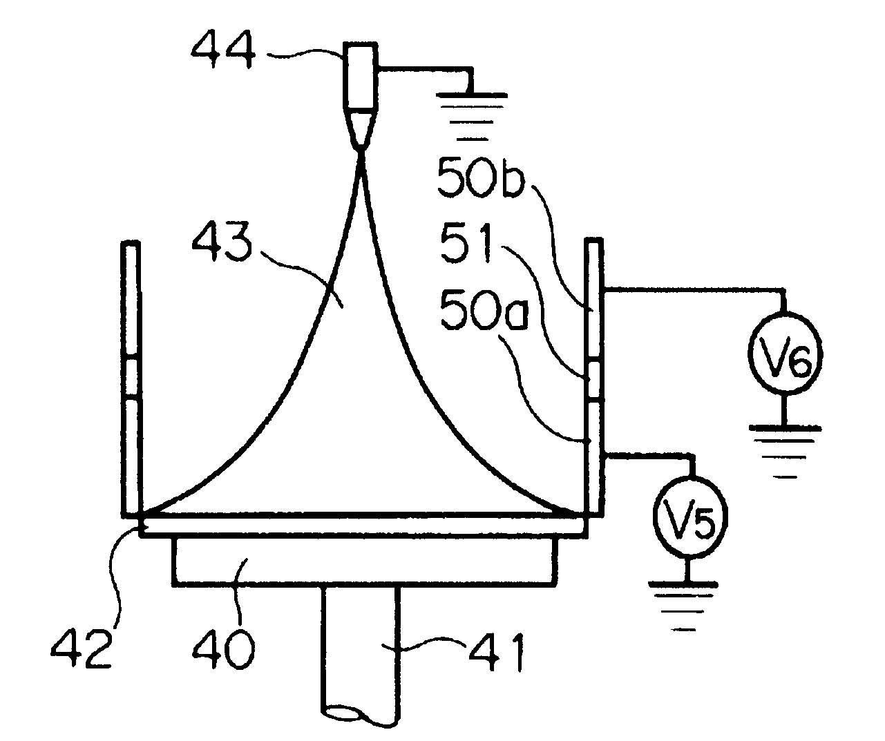
FIG. 8 illustrates a spin-coating apparatus in accordance with the third embodiment. Parts or elements that correspond to those of the spin-coating apparatus illustrated in FIG. 5 have been provided with the same reference numerals.
The spin-coating apparatus in accordance with the third embodiment includes a second electrode 48 embedded in the rotary table 40. The second electrode 48 is electrically connected to a power source 49. Similarly to the first to fourth power sources V.sub.1, V.sub.2, V.sub.3 and V.sub.4, the power source 49 applies a voltage having an electric polarity opposite to an electric polarity of particles of the chemical 43, to the second electrode 48.
In accordance with the spin-coating apparatus, the electrode 45 attracts the chemical 43 towards a periphery of the semiconductor substrate 42 to thereby uniformly spread the chemical 43 over the semiconductor substrate 42, and concurrently, the second electrode 48 attracts the chemical 43 towards a surface of the s...
PUM
| Property | Measurement | Unit |
|---|---|---|
| electric field | aaaaa | aaaaa |
| semiconductor | aaaaa | aaaaa |
| electric polarity | aaaaa | aaaaa |
Abstract
Description
Claims
Application Information
 - R&D
- Intellectual Property
- Life Sciences
- Materials
- Tech Scout
- Unparalleled Data Quality
- Higher Quality Content
- 60% Fewer Hallucinations
Browse by: Latest US Patents, China's latest patents, Technical Efficacy Thesaurus, Application Domain, Technology Topic, Popular Technical Reports.
© 2025 PatSnap. All rights reserved.Legal|Privacy policy|Modern Slavery Act Transparency Statement|Sitemap|About US| Contact US: help@patsnap.com


