
Multiple-port semiconductor memory device

a memory device and multi-port technology, applied in the direction of information storage, static storage, digital storage, etc., can solve the problems of large read time and line space consumption of operations

Inactive Publication Date: 2001-01-30
RENESAS ELECTRONICS CORP
View PDF6 Cites 74 Cited by
  • Summary
  • Abstract
  • Description
  • Claims
  • Application Information

AI Technical Summary

Problems solved by technology

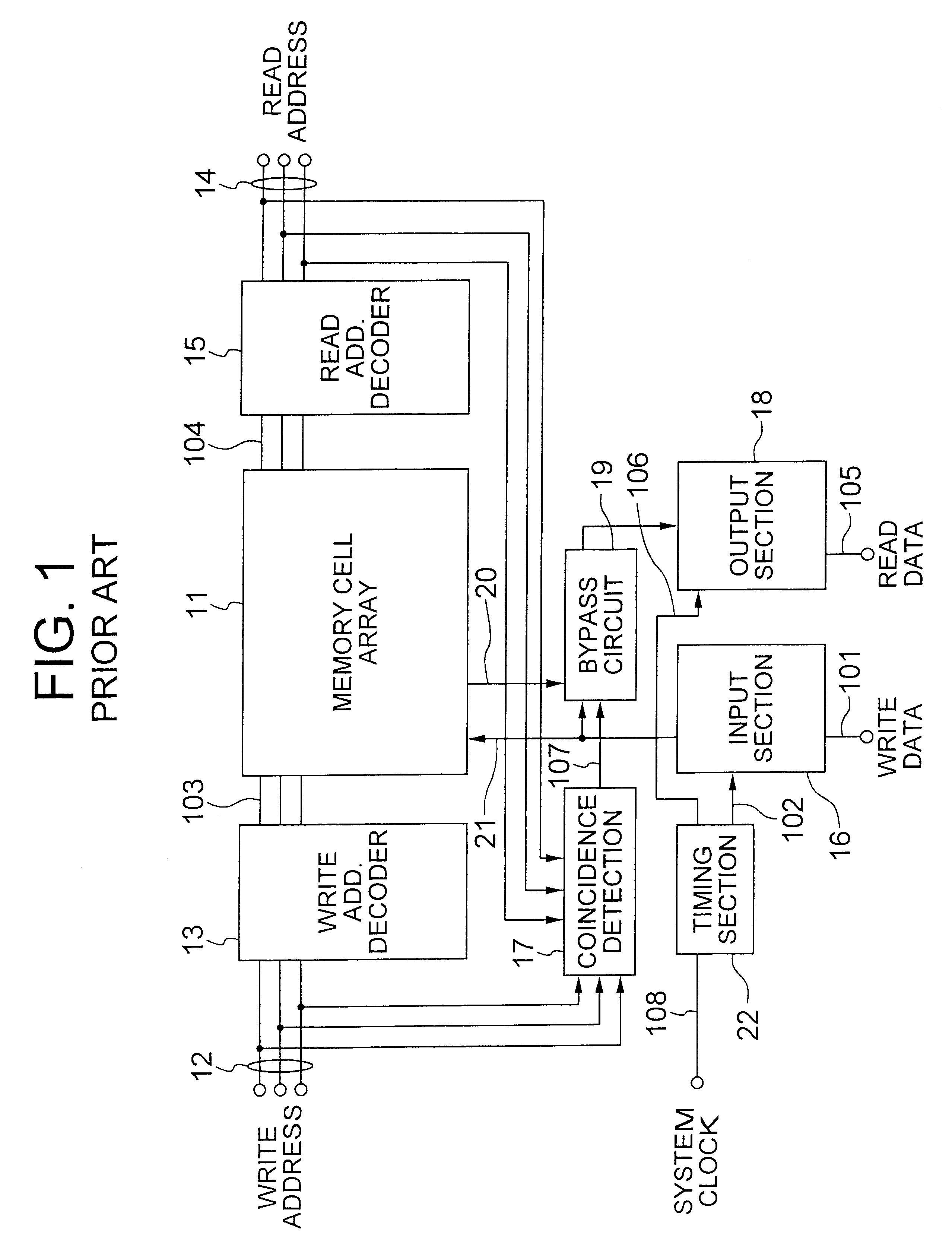
However, this operation consumes a larger read time compared to the ordinary read operation in a SRAM.
This problem is enhanced by the reduction of the line space in the current dual-port SRAM, wherein a coupling capacitance is increased more and more between adjacent bit lines.

Method used


Image

  • Multiple-port semiconductor memory device
  • Multiple-port semiconductor memory device
  • Multiple-port semiconductor memory device

Examples


Embodiment Construction

Now, the present invention is more specifically described with reference to accompanying drawings.

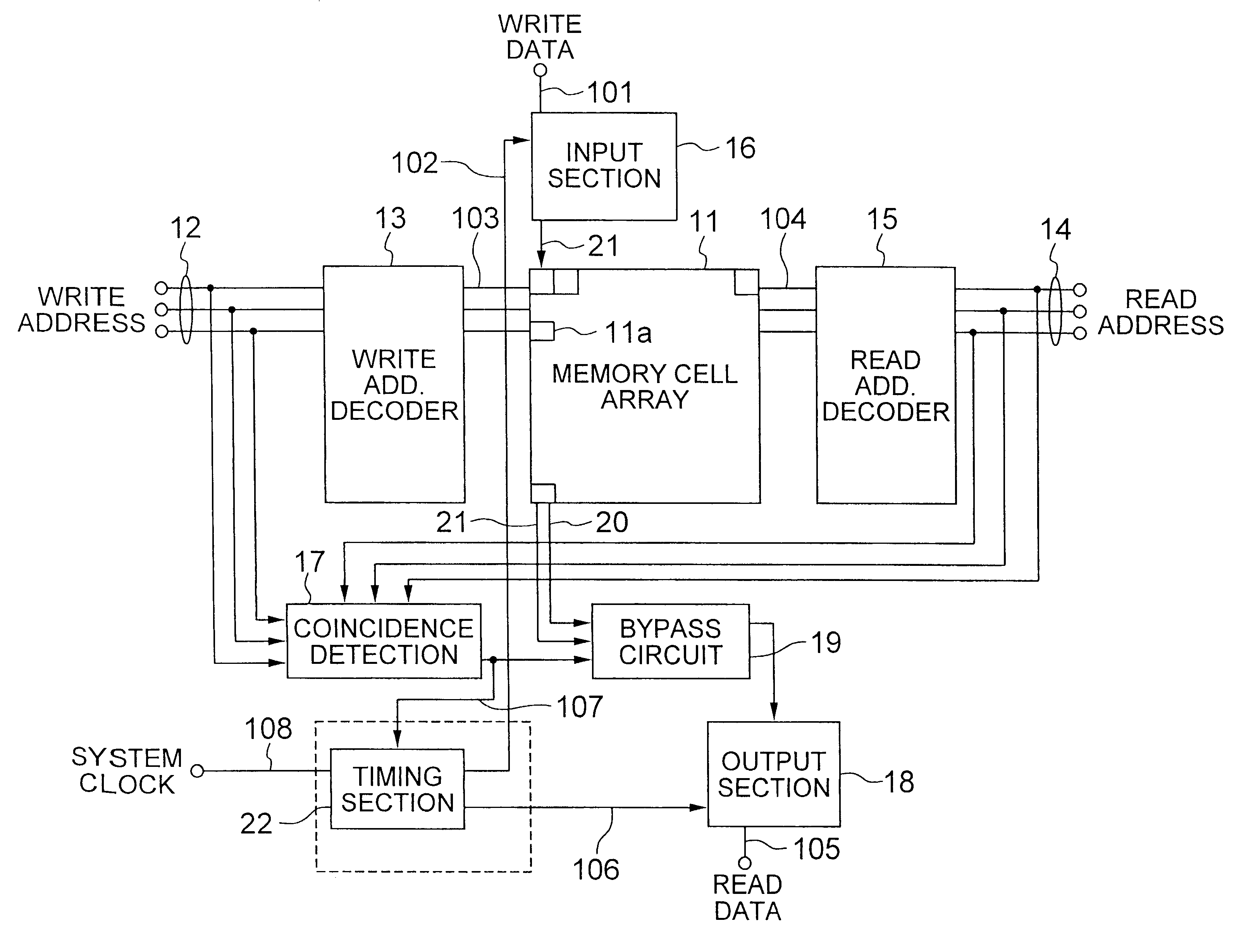
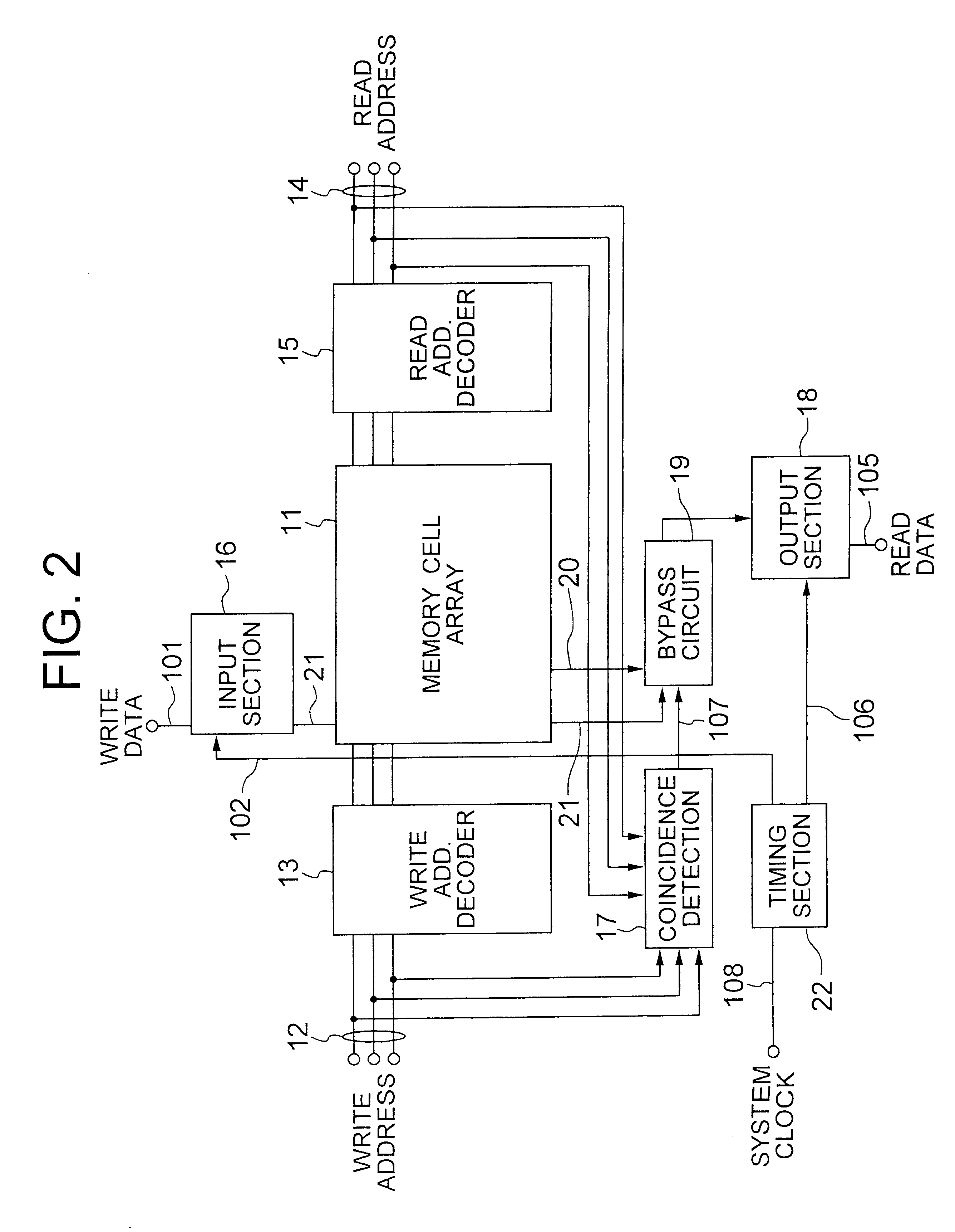
Referring to FIG. 5, a dual-port SRAM according to an embodiment of the present invention includes a memory cell array 11 including a plurality of memory cells arranged in a matrix, a write address decoder 13 for receiving write address through an input port address bus 12, a read address decoder 15 for receiving a read address through an output port address bus 14, an input section 16 for receiving a write data 101 to store the write data to the memory cell array 11, an output section 18 for delivering a read data 105 read from the memory cell array 11, a coincidence detection section (comparator) 17 for comparing the write address and the read address to deliver a coincidence signal 107 which is active upon detection of a coincidence therebetween, a bypass section 19 for receiving the read data from the memory cell array 11 through a pair of read bit lines 20 to deliver the read data ...


PUM


Abstract

A dual-port SRAM operates for read and write operations in a single clock cycle. The SRAM has a comparator for comparing the read address and the write address to detect a coincidence therebetween. A bypass circuit bypasses the write data as a read data upon detection of a coincidence, whereas a timing circuit delays the write control signal with respect to the read control signal upon detection of no coincidence. The timing control between the read operation and the write operation reduces signal interference between the write data and the read data and enables a higher speed operation of the computer system.

Description

(a) Field of the InventionThe present invention relates to a multiple-port semiconductor memory device and, more particularly, to a multiple-port semiconductor memory device, wherein a pair of data, for example, are concurrently read from and written in the memory cell array through an input port and an output port. The present invention also relates to a method for controlling such a-multiple-port semiconductor memory device.(b) Description of a Related ArtA multiple-port SRAM, typically known as a dual-port SRAM, is generally incorporated as a core macro-block in a LSI. In the general dual-port SRAM, if data are to be read from and written in a single memory cell (or the same address), both the read and write operations are conducted concurrently as in the case of different addresses. In this situation, the read data changes during the read operation from the old data, stored in the memory cell before the write operation, to the new data written into the memory cell after the writ...

Claims


Application Information

Patent Timeline
Patent Type & Authority Patents(United States)
IPC IPC(8): G11C8/16G11C7/10G11C8/00G11C11/413G11C11/41G11C11/4193
CPCG11C7/1045G11C8/16G11C11/413
Inventor OKITA, MUNEHISA
Owner RENESAS ELECTRONICS CORP
Learn More