
Semiconductor aggregate substrate and semiconductor device with fuse structure to prevent breakdown

a technology of semiconductor devices and aggregate substrates, applied in the direction of optics, transistors, instruments, etc., can solve the problems of electrostatic damage, electrostatic breakdown in the internal circuit, and harm to the semiconductor device after separation

Inactive Publication Date: 2000-12-05
SONY CORP
View PDF7 Cites 44 Cited by
  • Summary
  • Abstract
  • Description
  • Claims
  • Application Information

AI Technical Summary

Problems solved by technology

The residual connection pattern 14 is not only unnecessary but also harmful to the semiconductor device after separation.
Specifically, the connection pattern 14 acts as an antenna which can collect external static electricity, thereby causing electrostatic damage and electrostatic breakdown in the internal circuit.

Method used


Image

  • Semiconductor aggregate substrate and semiconductor device with fuse structure to prevent breakdown
  • Semiconductor aggregate substrate and semiconductor device with fuse structure to prevent breakdown
  • Semiconductor aggregate substrate and semiconductor device with fuse structure to prevent breakdown

Examples


Embodiment Construction

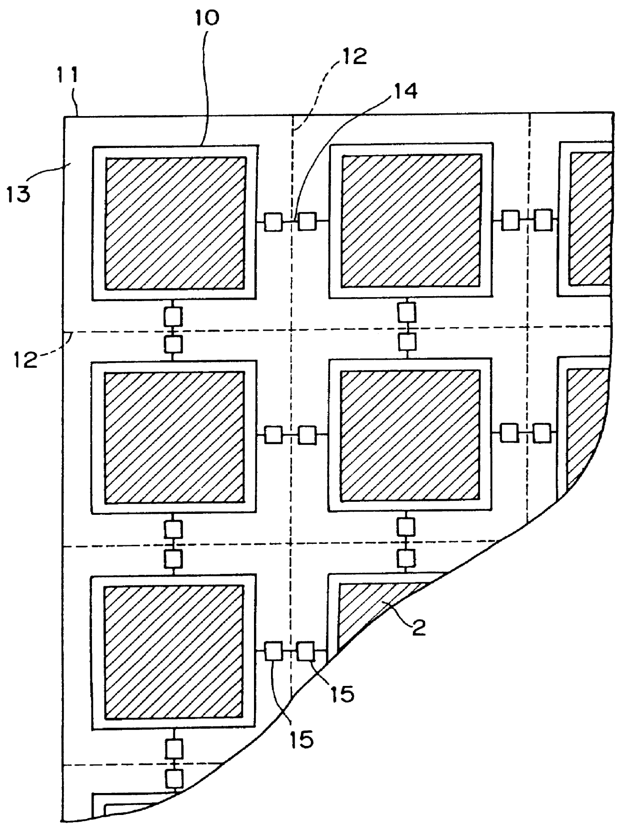
A preferred embodiment of the present invention will now be described in detail with reference to the accompanying drawings. As illustrated in FIG. 1, a semiconductor aggregate substrate is constituted by a wafer 11 made of, for example, a large rectangular quartz plate. A polycrystalline silicon thin film or the like is formed on the surface of the quartz wafer 11 to provide a device region. The wafer 11 has a plurality of segments 13 divided by predetermined vertical and horizontal division lines 12. A display active matrix circuit 2 is integrally formed in each of the segments 13. Guard ring patterns 10 are provided so that they surround the individual display active matrix circuits 2. The guard ring patterns 10 can be formed by patterning, for example, aluminum thin film used as a material for a wiring electrode and the like. The guard ring patterns 10 adjoining each other through the division lines 12 are commonly connected each other by a connection pattern 14. The connection ...


PUM

PropertyMeasurementUnit
semiconductoraaaaaaaaaa
gate widthaaaaaaaaaa
electric potentialaaaaaaaaaa

Abstract

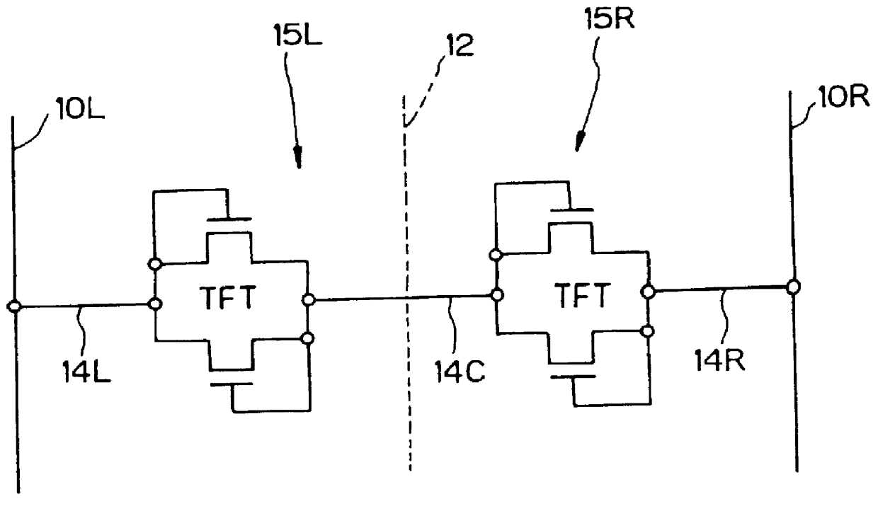
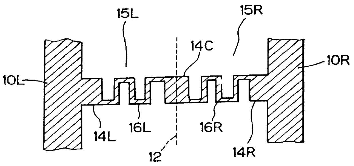
Electrostatic breakdown is avoided during fabrication of individual semiconductor devices using a semiconductor aggregate substrate. The semiconductor aggregate substrate is comprised of a large wafer. A plurality of sections are provided on the surface of the wafer, which are divided by division lines. A display active matrix circuit is integrally formed in each of the segments through normal IC production processing. Guard ring patterns are provided so that they surround the individual display active matrix circuits. A connection pattern is also provided for commonly connecting the guard ring patterns adjoining each other through the division lines. The connection pattern has opening structures for dealing with an external overcurrent on both sides of the division lines. The opening structures are constituted by, for example fuse patterns.

Description

1. Field of the InventionThe present invention relates to a semiconductor aggregate substrate and semiconductor devices and, more particularly, to an electrostatic charge protection device for a semiconductor aggregate substrate on which a multiplicity of display active matrix circuits are integrally formed. Additionally, the present invention relates to a guard ring structure for an active matrix circuit display.2. Description of the Related ArtFIG. 5 is a typical plan view showing an example of a conventional semiconductor device. This semiconductor device is a thin film type wherein a semiconductor thin film formed on an insulating substrate 1 is used as a device region. Display active matrix circuits 2 are integrally formed on the surface of the insulating substrate 1. A semiconductor device having such a configuration is used, for example, for liquid crystal display elements of an active matrix type. For example, an active matrix type liquid crystal display element is obtained ...

Claims


Application Information

Patent Timeline
Patent Type & Authority Patents(United States)
IPC IPC(8): H01L23/60H01L23/525H01L23/58H01L23/52G02F1/136G02F1/1345G02F1/1368H01L23/62H01L27/12H01L29/78H01L29/786
CPCH01L23/5256H01L23/60H01L23/62H01L2924/0002H01L2924/00
Inventor KOBAYASHI, MIKIYA
Owner SONY CORP
Learn More