Method and device of chemical mechanical polishing

a technology of mechanical polishing and chemical technology, applied in the field of semiconductors, can solve the problems of affecting the washing effect, the particle size and the adverse effect of the polishing process on the following fine polishing process

Pending Publication Date: 2022-03-31
ZING SEMICON CORP
View PDF3 Cites 0 Cited by
  • Summary
  • Abstract
  • Description
  • Claims
  • Application Information

AI Technical Summary

Benefits of technology

[0005]In the summary of the invention, a series of concepts in a simplified form is introduced, which will be described in further detail in the detailed description. This summary of the present invention does not intend to limit the key elements or the essential technical features of the claimed technical solutions, nor intend to limit the scope of the claimed technical solution.
[0006]To solve the problem in the conventional technology, the present application provides a method of chemical mechanical polishing (CMP) comprising: providing a semiconductor wafer to be subjected to polishing; conducting a CMP process to the wafer, wherein the wafer is on a first plane during the CMP process; conducting a hanging treatment, wherein, in the hanging treatment, the wafer is on a second plane above the first plane, the wafer is hanged to expose the lower surface, and the wafer is in rotation.

Problems solved by technology

The polishing particles and the byproduct particles in the stock polishing process adversely affect the following fine polishing process.
For another example, a washing process is conducted after the CMP process, but the washing effect is adversely affected by the polishing particles and the byproduct particles attached to the wafer surface.

Method used


Image

  • Method and device of chemical mechanical polishing
  • Method and device of chemical mechanical polishing
  • Method and device of chemical mechanical polishing

Examples


example 1

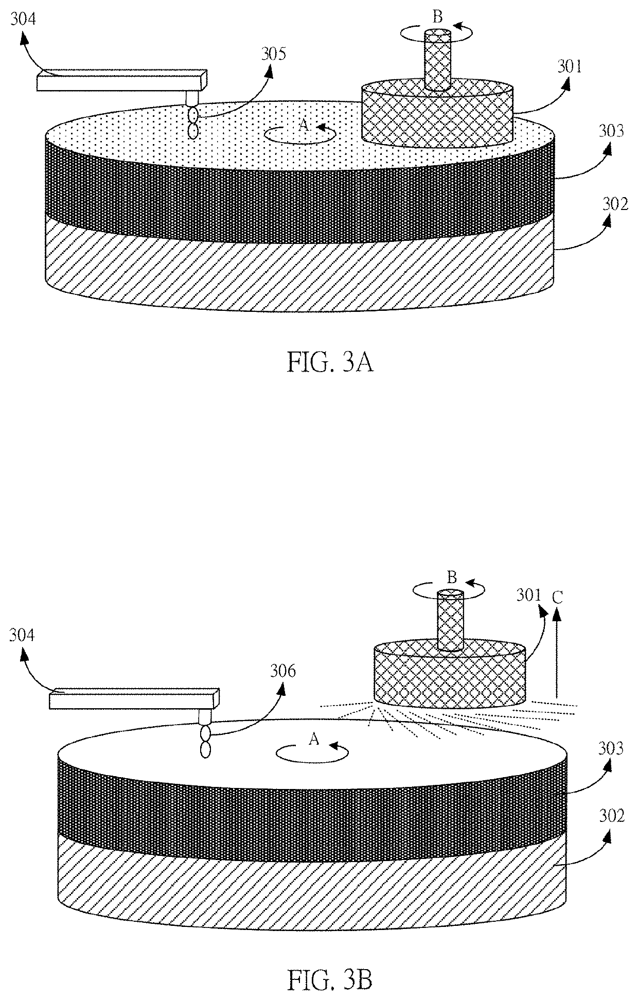
[0027]To solve the problem in the conventional technology, the present application provides a CMP method. The CMP method comprises providing a semiconductor wafer to be subjected to polishing; conducting a CMP process to the wafer, wherein the wafer is on a first plane during the CMP process; conducting a hanging treatment, wherein, in the hanging treatment, the wafer is on a second plane above the first plane, the wafer is hanged to expose the lower surface, and the wafer is in rotation.

[0028]Referring FIG. 2 and FIGS. 3A-3C, the CMP method of the present application is described illustratively. FIG. 2 shows a flow chart of the CMP process in accordance with an embodiment of the present application. FIGS. 3A-3C show a schematic view of the relative positions of the polishing pad and the wafer in the CMP process in accordance with an embodiment of the present application.

[0029]Firstly, referring FIG. 2, conducting Step S1: providing a wafer to be subjected to polishing.

[0030]The waf...

example 2

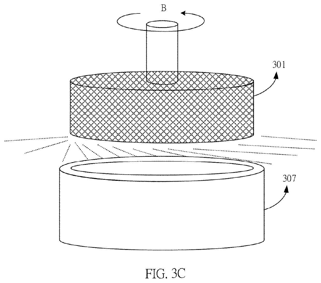
[0061]The present application provides a device of chemical mechanical polishing. The device comprises a polishing head for carrying a semiconductor wafer and driving a motion of the wafer. The motion comprises a first motion and a second motion. The CMP process is conducted during the first motion, and the polishing head is on a first plane during the CMP process. The hanging treatment is conducted during the second motion, and, in the hanging treatment, the wafer is on a second plane above the first plane. The wafer carried by the polishing head is hanged to expose the lower surface. During the hanging treatment, the polishing head rotates.

[0062]Referring to FIG. 3A-FIG. 3C, the device is illustratively described.

[0063]Referring to FIG. 3A, the CMP device comprises the polishing head 301 for carrying a semiconductor wafer (not shown), the polishing platform 302 for bearing the polishing pad 303, and the liquid supply device 304 for providing the polishing slurry 305 onto the polis...


PUM

PropertyMeasurementUnit
areaaaaaaaaaaa
rotation speedaaaaaaaaaa
semiconductoraaaaaaaaaa

Abstract

The present application provides a method and a device of chemical mechanical polishing (CMP). The method comprises providing a semiconductor wafer to be subjected to polishing; conducting a CMP process to the wafer, wherein the wafer is on a first plane; conducting a hanging treatment, wherein, in the hanging treatment, the wafer is on a second plane above the first plane, the wafer is hanged to expose the lower surface, and the wafer is in rotation. According to the present application, the hanging treatment can remove the slurry, the polishing particles and byproducts from the wafer surface, therefore, it prevents from the adverse effects caused by the polishing particles and byproducts on the wafer in the following process.

Description

BACKGROUND OF THE INVENTION1. Field of the Invention[0001]The present application relates to the technical field of semiconductor, in particular to a method and a device of chemical mechanical polishing.2. Description of the Related Art[0002]In the semiconductor manufacture process, from wafer production to device formation, chemical mechanical polishing (CMP) process may be conducted for the semiconductor wafer for several times. Since the applied CMP slurry carries a lot of particles and the byproducts as well as the debris are produced during the CMP process, these materials are attached to the surface of the semiconductor wafer. As shown in FIG. 1, the polishing head 101 carries the semiconductor wafer 100 to conduct CMP process on a surface of a polishing pad 102. A slurry 103 is provided to the surface of the polishing pad 102. The slurry 103 contains polishing particles P1. The wafer 100 reacts with the slurry 103 to form byproduct particles P2. These particles P1 and P2 usua...

Claims


Application Information

Patent Timeline
Patent Type & Authority Applications(United States)
IPC IPC(8): B24B37/04H01L21/461
CPCB24B37/04H01L21/461B24B1/00B24B29/02H01L21/30625H01L21/67092H01L21/02024H01L21/02052H01L21/02065H01L21/02074H01L21/31053H01L21/3212H01L21/67017H01L21/67023H01L21/67051H01L21/6715
Inventor SHA, YOUHEXIE, YUE
Owner ZING SEMICON CORP
Why Eureka
Try Eureka