Semiconductor package

a technology of semiconductor chips and components, applied in the direction of secondary cell servicing/maintenance, battery overheat protection, safety/protection circuits, etc., can solve problems such as signal errors in circuit elements, and achieve the effects of minimizing the signal error of the circuit element due to a piezoelectric phenomenon, and reducing the pressure applied to the circuit element formed in the semiconductor chip

Pending Publication Date: 2022-03-10
SILICON WORKS CO LTD
View PDF0 Cites 0 Cited by
  • Summary
  • Abstract
  • Description
  • Claims
  • Application Information

AI Technical Summary

Benefits of technology

[0012]According to an embodiment of the present invention, a pressure-reducing layer is formed on a semiconductor chip, and thus pressure applied to a circuit element formed in the semiconductor chip can be reduced, and a signal error of the circuit element due to a piezoelectric phenomenon can be minimized. In addition, according to an embodiment of the present invention, a buffer layer is further provided between the semiconductor chip and the pressure-reducing layer, and thus the pressure applied to the circuit element formed in the semiconductor chip can be minimized, and the signal error of the circuit element due to the piezoelectric phenomenon can be minimized.

Problems solved by technology

More specifically, when a high pressure is applied to the circuit element, a signal error may occur in the circuit element due to occurrence of a piezoelectric phenomenon.

Method used


Image

  • Semiconductor package
  • Semiconductor package
  • Semiconductor package

Examples


Embodiment Construction

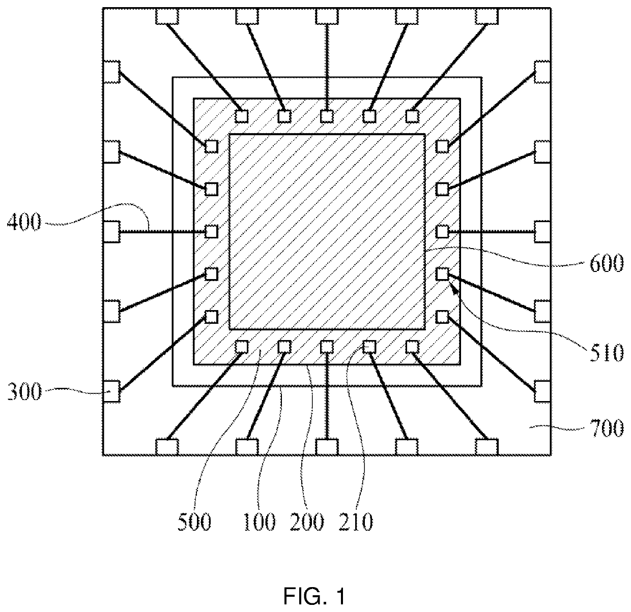
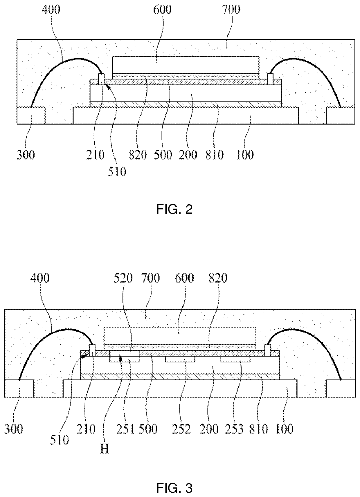
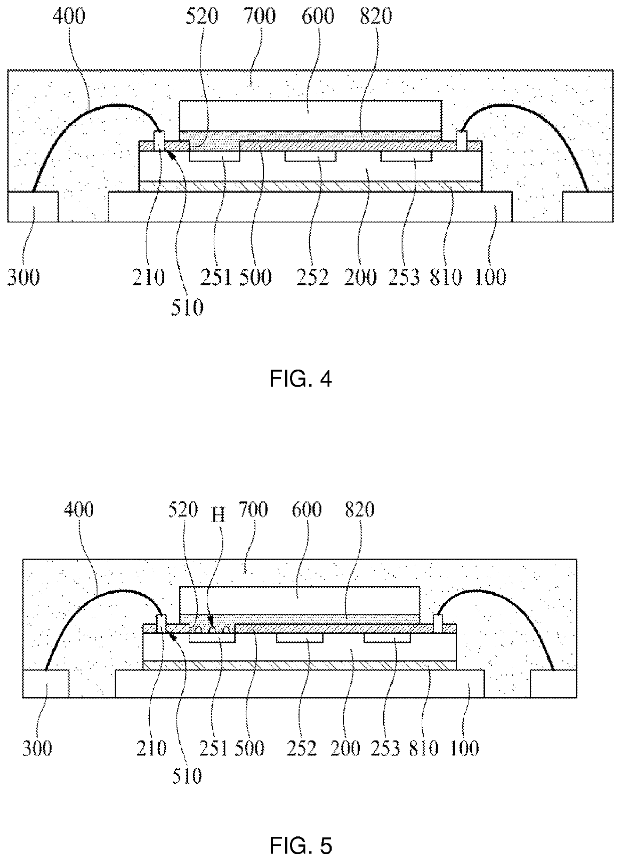
[0020]Throughout the specification, the same reference numerals refer to substantially the same components. In the following description, when it is determined that a detailed description of a well-known function or configuration related to the present invention may unnecessarily obscure the gist of the present invention, the detailed description thereof is omitted. In addition, the component names used in the following description may be selected in consideration of the ease of writing the specification and may be different from the actual product part names.

[0021]Advantages and features of the present invention and methods for achieving them will be apparent with reference to the embodiments described below in detail with reference to the accompanying drawings. However, the present invention is not limited to the embodiments disclosed below but will be implemented in various forms, and only the embodiments of the present invention make the disclosure of the present invention compl...


PUM

PropertyMeasurementUnit
thicknessaaaaaaaaaa
pressureaaaaaaaaaa
thicknessaaaaaaaaaa

Abstract

The present invention provides a semiconductor package, comprising: a support part; a semiconductor chip provided on the support part and including a plurality of signal pads; a buffer layer provided on the semiconductor chip; an adhesive layer provided on the buffer layer; a pressure-reducing layer provided on the adhesive layer; and a mold layer provided on the pressure-reducing layer.

Description

TECHNICAL FIELD[0001]The present invention relates to a semiconductor package.BACKGROUND ART[0002]A semiconductor package is mounted on a substrate and manufactured in various types of semiconductor devices.[0003]Such a semiconductor package includes a semiconductor chip and a mold layer formed on the semiconductor chip.[0004]A large number of circuit elements that perform a predetermined function are formed in the semiconductor chip.[0005]The mold layer is formed on an upper surface of the semiconductor chip to protect the semiconductor chip. The mold layer is formed on the upper surface of the semiconductor chip under high pressure, and therefore, a high pressure is applied to the semiconductor chip in a process of forming the mold layer.[0006]However, when a high pressure is applied to the semiconductor chip during the manufacturing process, the high pressure is transmitted to the circuit element formed in the semiconductor chip, and thus the electrical characteristics of the cir...

Claims


Application Information

Patent Timeline
Patent Type & Authority Applications(United States)
IPC IPC(8): H01L23/00H01L23/495H01L23/31H02J7/00
CPCH01L23/562H02J7/0014H01L23/3107H02J7/007182H01L24/05H01L24/48H01L2224/04042H01L2224/32245H01L24/32H01L2224/48247H01L2224/49171H01L24/49H01L2224/48091H01L2224/73265H01L24/73H02J7/0048H02J7/005H02J7/00302H02J7/00306H02J7/00309H01L23/49568H01L2924/181H01L25/18H01M10/425H01L23/49575H01L23/49541H01M2010/4271H01M10/482H01M10/486Y02E60/10H01L2924/00012H01L2924/00014H01L2924/00
Inventor SONG, MYOUNG SU
Owner SILICON WORKS CO LTD
Why Eureka
Try Eureka