Arrangement structure for electrode of micro LED

a technology of arrangement structure and electrode, which is applied in the direction of basic electric elements, electrical equipment, semiconductor devices, etc., can solve the problems of inconvenient alignment and attaching of common led, increased price of micro led, and difficulty in mass production, so as to achieve rapid and easy manufacturing process

Pending Publication Date: 2022-01-27
RYUJIN LAB INC
View PDF0 Cites 4 Cited by
  • Summary
  • Abstract
  • Description
  • Claims
  • Application Information

AI Technical Summary

Benefits of technology

The patent text proposes an arrangement structure for the electrodes of a micro LED that ensures driving without any problems regardless of the rotation or changes in the left, right, upper, or lower sides of the LED. This is achieved by maintaining symmetry between the LED anode element and cathode element and connecting them in a single circular structure. Additionally, the text suggests that if the LED anode element and cathode element are fixedly attached to each other without alignment, the driving may still be performed without problems. This simplifies the manufacturing process and enables easy and rapid attachment between the electrodes.

Problems solved by technology

However, at the current technical level, such micro LED displays have a problem in that it takes a lot of time to place LEDs on a PCB or TFT substrate, so that the price thereof is increased and it is difficult to perform the mass production thereof.
Accordingly, there is the inconvenience of aligning and attaching the common LED.
Accordingly, a problem arises in that more time is consumed.
This related art has a problem in that it is cumbersome and takes a lot of time to manufacture a micro LED device because it is necessary to erect a micro LED device and align and fixedly attach the micro LED to an electrode in a one-to-one correspondence.

Method used


Image

  • Arrangement structure for electrode of micro LED
  • Arrangement structure for electrode of micro LED
  • Arrangement structure for electrode of micro LED

Examples


Embodiment Construction

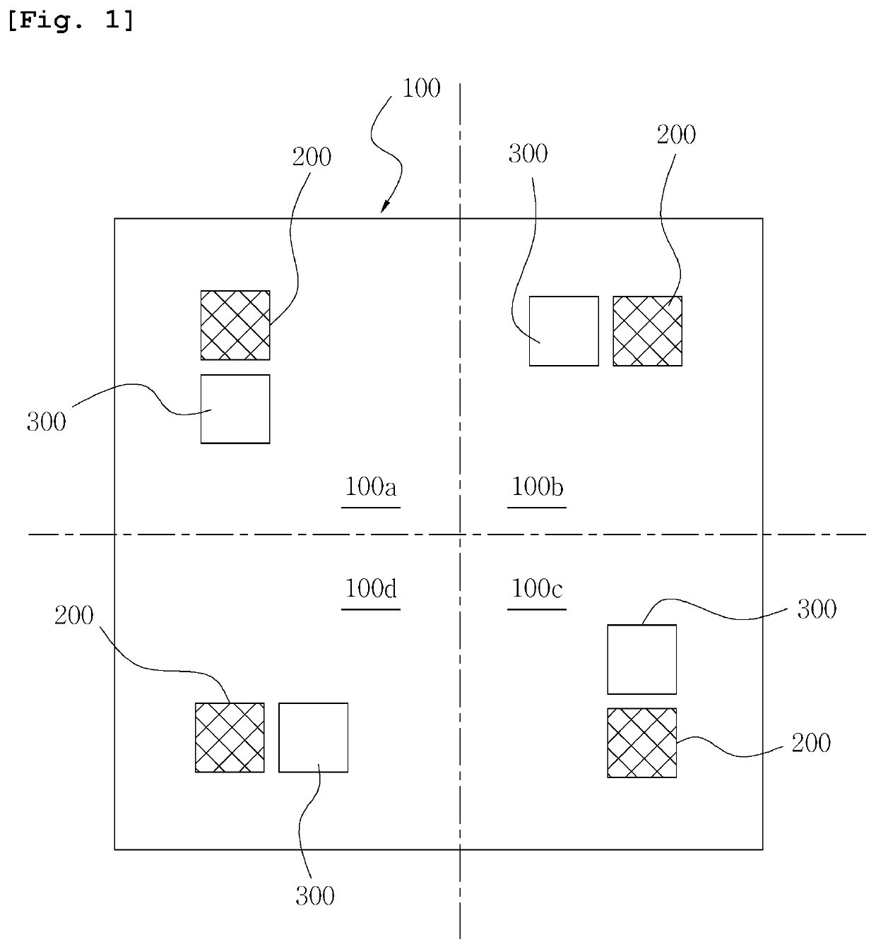
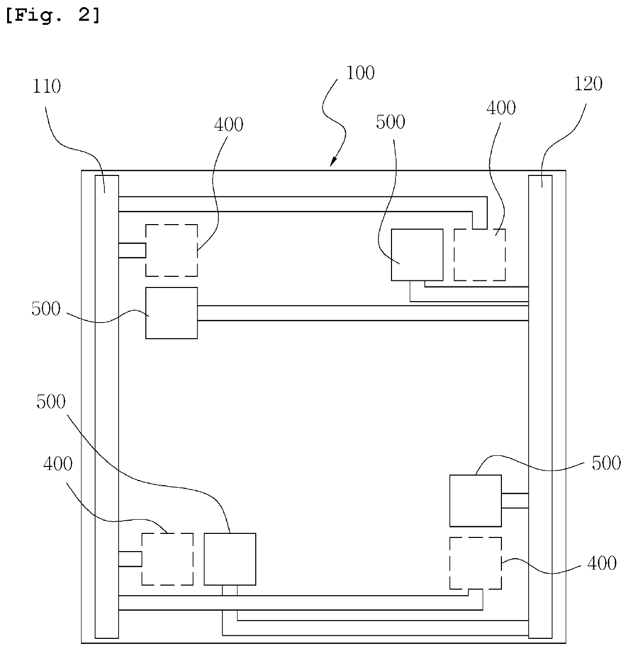
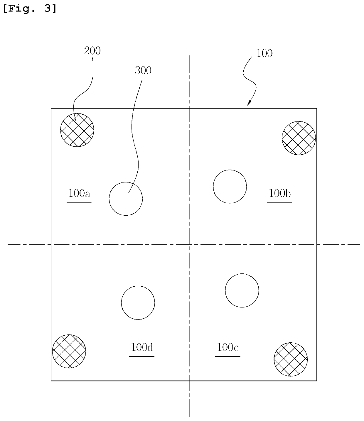
[0030]Various embodiments will be described in detail below with reference to the accompanying drawings. The following embodiments may be modified to various different forms and then practiced. In order to more clearly illustrate features of the embodiments, detailed descriptions of items which are well known to those having ordinary skill in the art to which the following embodiments pertain will be omitted. Furthermore, in the drawings, portions unrelated to descriptions of the embodiments will be omitted. Throughout the specification, like reference symbols will be assigned to like portions.

[0031]Throughout the specification, when one component is described as being “connected” to another component, this includes not only a case where the one component is ‘directly connected’ to the other component but also a case where the one component is ‘connected to the other component with a third component arranged therebetween.’ Furthermore, when one portion is described as “including” on...


PUM

PropertyMeasurementUnit
sizeaaaaaaaaaa
currentaaaaaaaaaa
areaaaaaaaaaaa

Abstract

Proposed is an arrangement structure for the electrodes of a micro LED that may perform driving without any problems even when an anode and a cathode constituting parts of the electrodes of a micro LED are rotated and thus the left, right, upper and / or lower sides thereof are changed. The arrangement structure includes: a substrate having an anode and a cathode; an LED anode element fixedly attached to the substrate, and configured to form an anode among electrodes of an LED device; an LED cathode element fixedly attached to the substrate, and configured to form a cathode among the electrodes of the LED device; an anode application element configured to apply a current while connecting the LED anode element to the anode of the substrate; and a cathode application element configured to apply a current while connecting the LED cathode element to the cathode of the substrate.

Description

TECHNICAL FIELD[0001]The embodiments disclosed herein relate to the design of the directions of electrode elements for the driving of a micro light-emitting diode (LED), the design of a driving substrate, and an arrangement structure for the electrodes of a micro LED formed by fixedly attaching the electrode elements. BACKGROUND ART[0002]In general, a micro LED display refers to a display using micro LEDs having a sire that is about 1 / 10 of the size of existing LEDs.[0003]Such a micro LED display implies using a substrate, in which significantly small LEDs are embedded, as a display. As a commonly used definition, a micro LED display refers to a display having an element size of 100 μm or less in each of length and width.[0004]However, in order for a micro LED display to be used in small devices such as smartphone displays, it must range from 5 to 10μm. 100 μm is 0.1 mm, which is only 254 PPI in terms of PPI, so that it is much inferior to an OLED method.[0005]Existing LED displays ...

Claims


Application Information

Patent Timeline
Patent Type & Authority Applications(United States)
IPC IPC(8): H01L33/38H01L27/15
CPCH01L33/387H01L27/156H01L33/62H01L25/167H01L25/0753
Inventor PARK, SEONG JINLEE, HONG JOOKIM, KIHYUNG
Owner RYUJIN LAB INC
Why Eureka
Try Eureka