Pixel structure and liquid crystal display panel

a liquid crystal display panel and pixel structure technology, applied in the field of displays, can solve the problems of weakness of liquid crystal display in high-end products, achieve the effects of improving optical difference, increasing viewing angles, and reducing light transmittance or liquid crystal efficiency

Inactive Publication Date: 2021-10-28
SHENZHEN CHINA STAR OPTOELECTRONICS SEMICON DISPLAY TECH CO LTD
View PDF0 Cites 0 Cited by
  • Summary
  • Abstract
  • Description
  • Claims
  • Application Information

AI Technical Summary

Benefits of technology

[0016]A pixel structure of the present invention is configured in combination with multi-domain vertical alignment architecture, and provides ITO electrode structures for four different domains according to a main pixel area and a subpixel area each having a voltage difference and light efficiency different from each other. By reducing an angle of electrode slits after angle adjustment of slits, light transmittance or liquid crystal efficiency is reduced at a front viewing angle. At this time, a projection of liquid crystal components seen from left and right sides of a display panel at a wide viewing angle is less different from being seen at the front viewing angle, thereby improving an optical difference between the two viewing angles, and achieving a purpose of increasing viewing angles, as well as improving display performance at different viewing angles, and thereby to effectively overcome a problem of color shift at a wide viewing angle in prior art.

Problems solved by technology

However, arrangement of slit structures of conventional pixel electrodes can only provide certain, limited wide viewing angles, giving rise to a weakness of liquid crystal displays in high-end products.

Method used


Image

  • Pixel structure and liquid crystal display panel
  • Pixel structure and liquid crystal display panel
  • Pixel structure and liquid crystal display panel

Examples


Embodiment Construction

[0023]The following embodiments are referring to the accompanying drawings for exemplifying specific implementable embodiments of the present invention. Directional terms described by the present invention, such as upper, lower, front, back, left, right, inner, outer, side, etc., are only directions by referring to the accompanying drawings, and thus the used directional terms are used to describe and understand the present invention, but the present invention is not limited thereto.

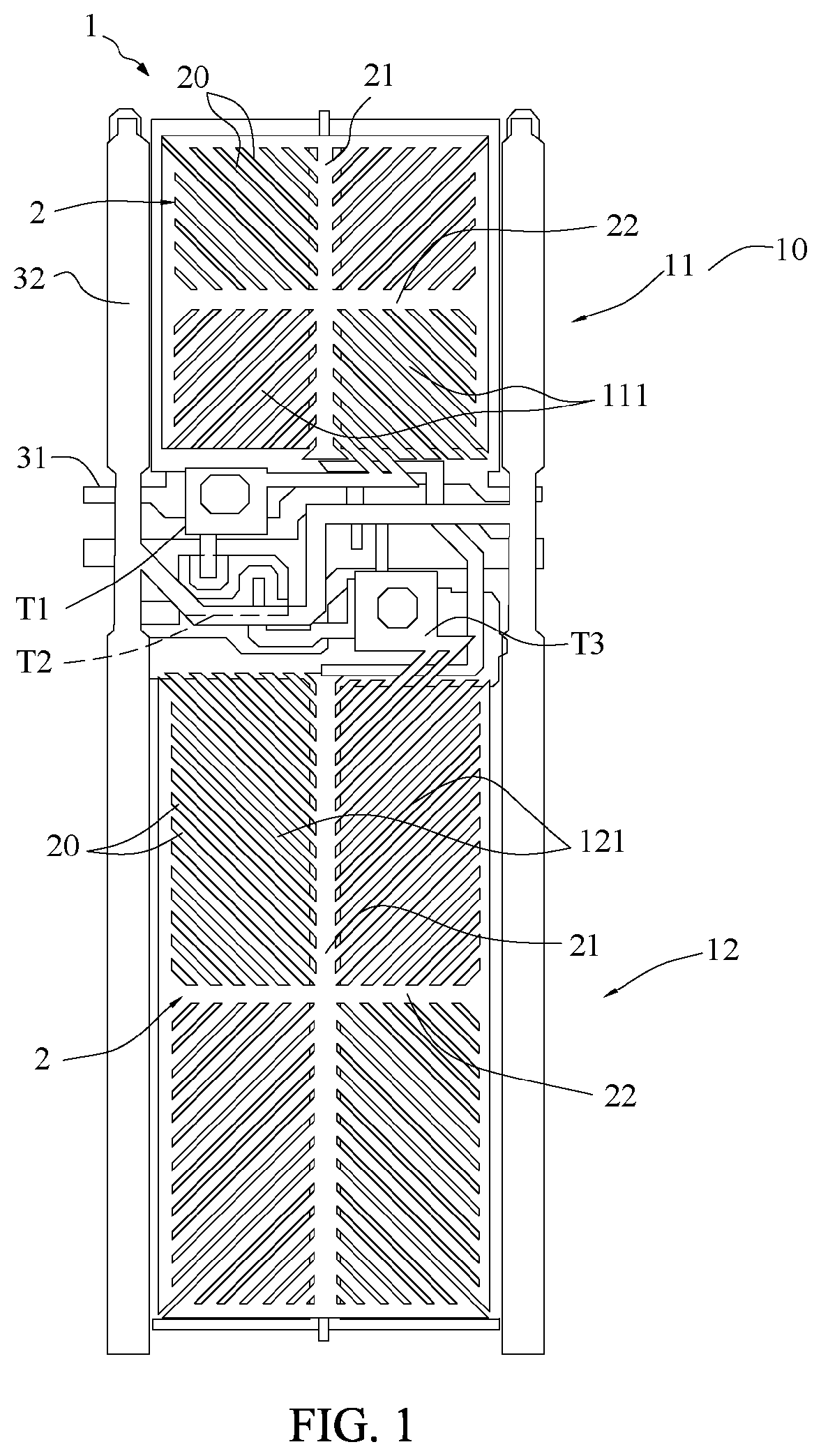
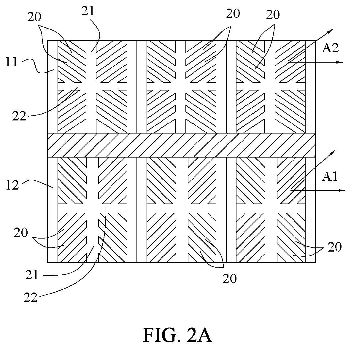
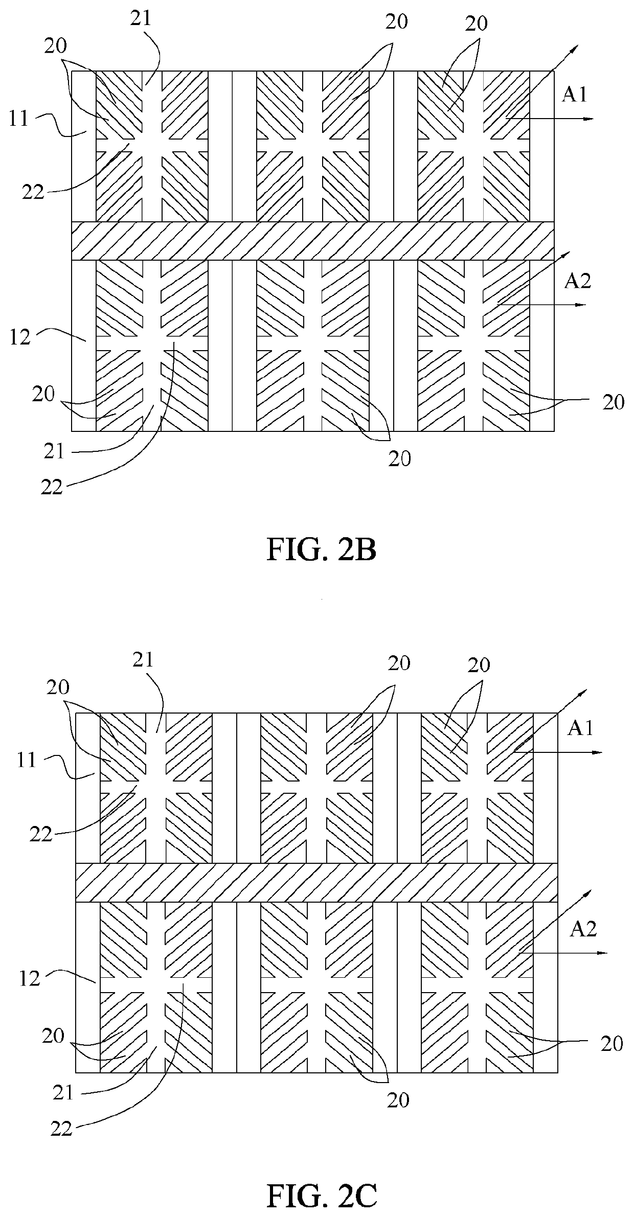
[0024]The present invention relates to a pixel structure of a liquid crystal display panel, and particularly, to a pixel structure of a multi-domain vertical alignment liquid crystal display. FIG. 1 is a schematic structural view of a pixel structure of a preferable embodiment of the present invention, wherein a number of the pixel structure described below is one as an example. The present invention provides a pixel structure 1 arranged on a substrate 101 (as shown in FIG. 6). The pixel structure includ...


PUM

PropertyMeasurementUnit
angleaaaaaaaaaa
angleaaaaaaaaaa
angleaaaaaaaaaa

Abstract

A pixel structure is arranged on a substrate, and includes a pixel area disposed on the substrate. The pixel area is defined with a long axis and a short axis and includes a main pixel area and a subpixel area. A plurality of pixel electrodes are disposed on the main pixel area and the subpixel area. The pixel electrodes each include a plurality of slits spaced apart from and parallel with each other. The slits located in at least one of the main pixel area and the subpixel area are disposed at a first angle with respect to the short axis or the long axis, and the first angle is less than 45 degrees.

Description

BACKGROUND OF INVENTION1. Field of Invention[0001]The present invention relates to a technical field of displays, and particularly to, a pixel structure and a liquid crystal display panel.2. Related Art[0002]Display technology development is ever-changing. Liquid crystal displays have advantages of low voltage operation, no radiation scattering, being light weight, and being small-sized. They have been widely used in markets for years, and are still the mainstream of displays. Currently, liquid crystal display technologies that can meet requirements of wide viewing angles include twisted nematic (TN) liquid crystals with wide viewing angle films, in-plane switching (IPS) liquid crystal displays, multi-domain vertical alignment (MVA) liquid crystal displays, and so on.[0003]Conventional liquid crystal display panels includes array substrates and color filters (or color filter substrates) fabricated in a front-stage array process, and liquid crystals injected in the array substrates a...

Claims


Application Information

Patent Timeline
Patent Type & Authority Applications(United States)
IPC IPC(8): G02F1/1343G02F1/1368G02F1/1362
CPCG02F1/134309G02F1/136286G02F1/1368G02F1/13624G02F1/134345
Inventor CAO, WU
Owner SHENZHEN CHINA STAR OPTOELECTRONICS SEMICON DISPLAY TECH CO LTD
Why Eureka
Try Eureka