
Array substrate and display panel

a technology of array substrate and display panel, which is applied in the direction of electrical equipment, semiconductor devices, instruments, etc., can solve the problems of abnormal display panel and reduce product yield, and achieve the effects of reducing the deformation of the array substrate caused by cutting and splintering, preventing the breakage of the electrically conductive line, and increasing the hardness of the film layer structure of the region

Active Publication Date: 2021-07-22
WUHAN CHINA STAR OPTOELECTRONICS TECH CO LTD
View PDF0 Cites 0 Cited by
  • Summary
  • Abstract
  • Description
  • Claims
  • Application Information

AI Technical Summary

Benefits of technology

The patent describes a method of increasing the hardness of a semiconductor device by adding a metal pattern between the substrate and electrically conductive lines. This helps to reduce deformation of the substrate during cutting and improvement in product yields is achieved. In simple terms, this method improves the strength of the semiconductor device.

Problems solved by technology

A metal trace of the film layer structure is irreversibly broken because of deformation, causing the display panel to be abnormal, and reducing product yields.

Method used


Image

  • Array substrate and display panel
  • Array substrate and display panel

Examples


Embodiment Construction

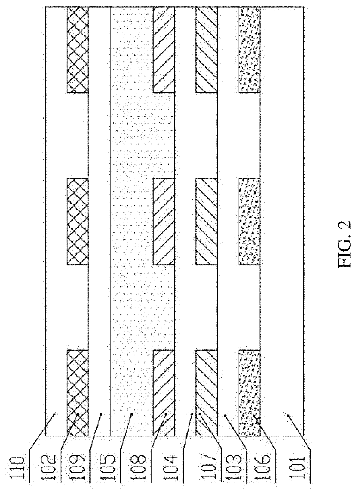
[0051]The description of each embodiment below refers to respective accompanying drawing(s), so as to illustrate exemplarily specific embodiments of the present disclosure that may be practiced. Directional terms mentioned in the present disclosure, such as “upper”, “lower”, “front”, “back”, “left”, “right”, “inner”, “outer”, “side”, etc., are only directions by referring to the accompanying drawings, and thus the used directional terms are used to describe and understand the present disclosure, but the present disclosure is not limited thereto. In the drawings, structurally similar units are labeled by the same reference numerals.

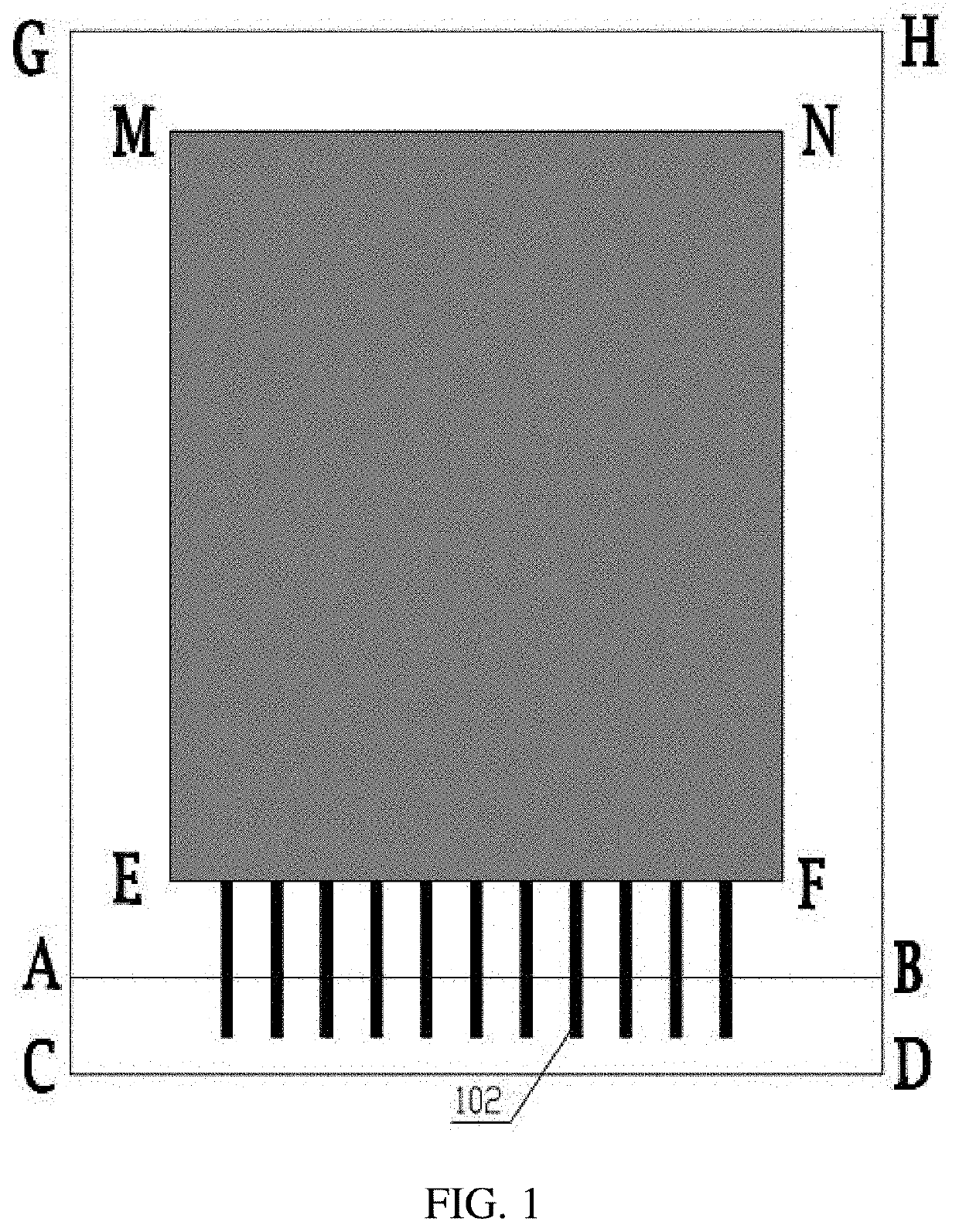
[0052]FIG. 1 is a top-view diagram of an array substrate in accordance with an embodiment of the present disclosure. The array substrate includes a first region and a second region. An area corresponding to the first region is a region MNFE.

[0053]In the present embodiment, the first region corresponds to a display region of a display panel. The second regi...


PUM

PropertyMeasurementUnit
electrically conductiveaaaaaaaaaa
response speedaaaaaaaaaa
brightnessaaaaaaaaaa

Abstract

An array substrate and a display panel are provided. The array substrate includes a first region and a second region. The first region corresponds to a display region of the display panel. The second region corresponds a non-display region of the display panel. The second region includes a substrate and an electrically conductive line formed on the substrate. The second region further includes at least one metal pattern formed between the substrate and the electrically conductive line.

Description

FIELD OF INVENTION[0001]The present disclosure relates to a technical field of flat panel displays, and more particularly to an array substrate and a display panel.BACKGROUND OF INVENTION[0002]Liquid crystal displays (LCDs) are a type of flat panel displays widely used. LCDs mainly modulate light field intensities of backlight sources through liquid crystal switches, to realize image display. LCD display devices include thin film transistor (TFT) devices. Each liquid crystal pixel on a TFT-LCD display is driven by thin film transistors integrated therein. Therefore, TFT-LCD displays have advantages of high response speed, high brightness, high contrast, small size, low power consumption, no radiation, etc., and dominate a current display market.[0003]In the related art, based on cost considerations, an array substrate manufactured and bonded to a color film substrate needs to be cut into a plurality of display panels of equal size. A display panel includes an array substrate cutting...

Claims


Application Information

Patent Timeline
Patent Type & Authority Applications(United States)
IPC IPC(8): H01L27/12
CPCH01L27/1244H01L27/1262G02F1/133516G02F1/1362G02F1/1368H01L27/124G02F1/1345
Inventor CAO, ZHIHAO
Owner WUHAN CHINA STAR OPTOELECTRONICS TECH CO LTD
Learn More