Organic el display device and manufacturing method therefor
a technology of organic el and display devices, which is applied in the direction of static indicating devices, organic semiconductor devices, instruments, etc., can solve the problems of uneven surface production, and achieve the effects of stable connection, low resistance, and elimination of variations in connection resistan
- Summary
- Abstract
- Description
- Claims
- Application Information
AI Technical Summary
Benefits of technology
Problems solved by technology
Method used
Image
Examples
example 1
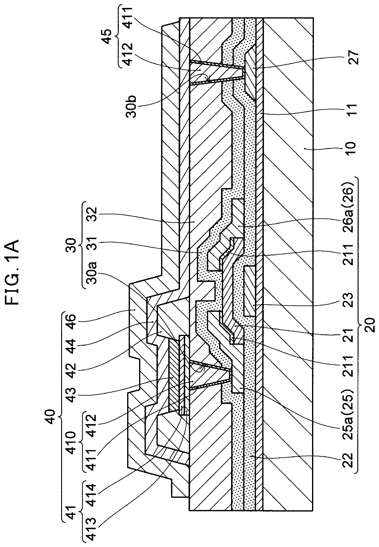
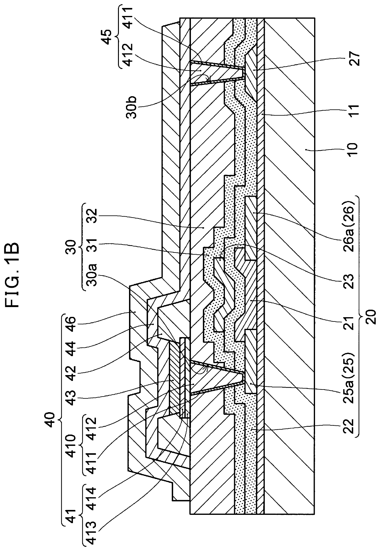
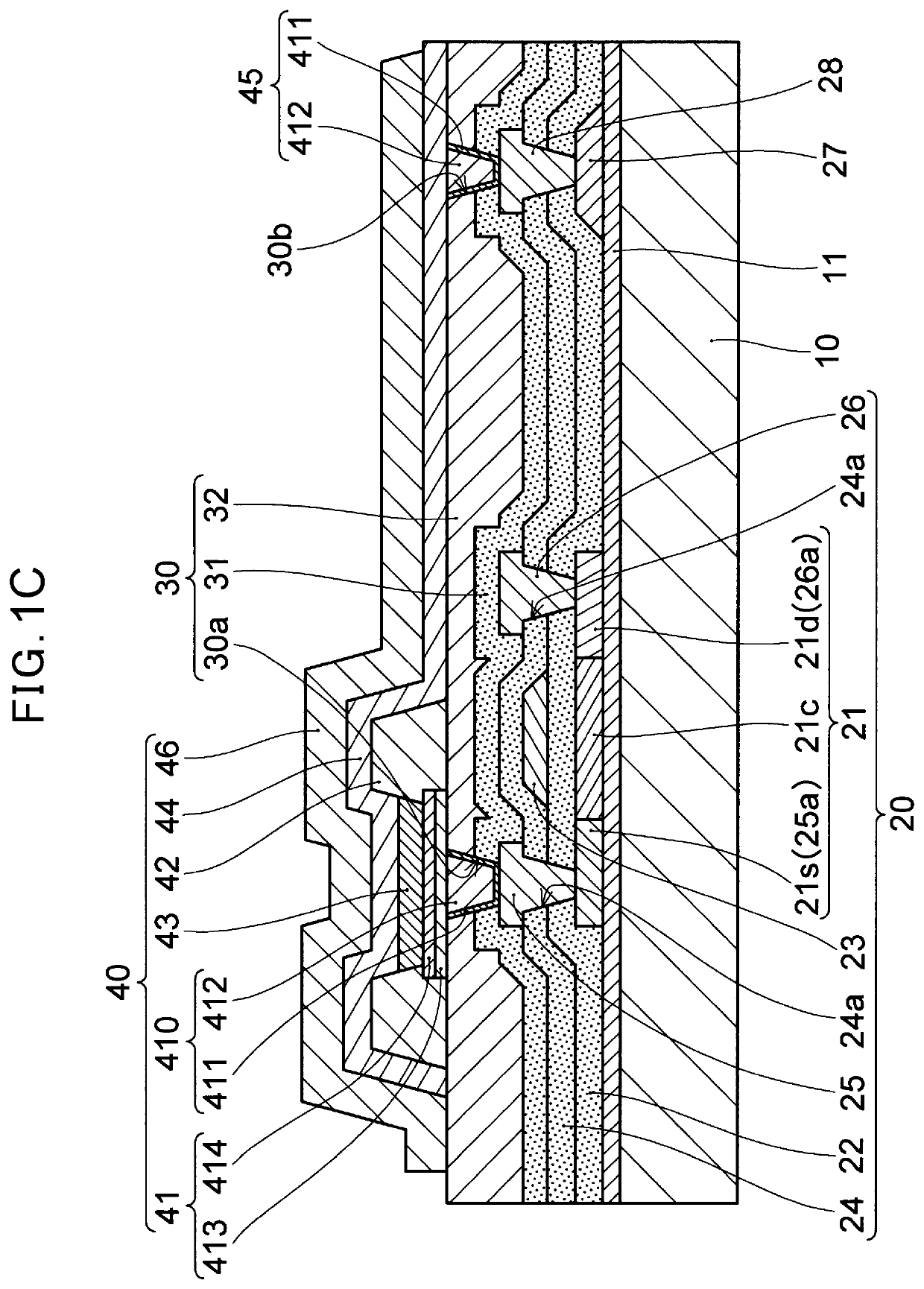
[0074]Next, a manufacturing method of the organic-EL display apparatus shown in FIG. 1A is explained with reference to flowcharts in FIGS. 4A and 4B and views of the manufacturing process in FIGS. 5A to 5G.
[0075]First, as shown in the flowchart in FIG. 4A, and in FIG. 5A, a drive circuit comprising a TFT 20 is formed over a substrate 10 (51 in FIG. 4A). Specifically, as shown in the flowchart in FIG. 4B, a base coat layer 11 is formed on the substrate 10. The base coat layer 11 is formed by forming an SiO2 layer to a thickness of approximately 500 nm, forming thereon an SiNx layer to a thickness of approximately 50 nm to deposit an underlayer, and depositing further thereon an SiO2 layer to a thickness of approximately 250 nm as an overlayer thereof, using plasma CVD, for example (S11 in FIG. 4B).
[0076]Thereafter, wirings such as a gate electrode 23, a cathode wiring 27, and the other gate wiring and signal wiring are formed on a surface of the base coat layer 11 by forming a metal ...
example 2
[0093]In the manufacturing method of according to Example 1 being shown in FIGS. 4A and 4B, and FIGS. 5A to 5G, while the inorganic insulating layer 31 and the organic insulating layer 32 are continuously formed and the contact hole 30a is collectively formed with respect to the planarizing layer 30, as the organic insulating layer 32, the organic insulating layer 32 comprising a photosensitive organic material comprising a photopolymerization initiator can be formed, the inorganic insulating layer 31 can be formed, and then, the first contact hole 30a1 can be formed, and thereafter, the organic insulating layer 32 having a photosensitivity can be formed, and the second contact hole 30a2 can be formed by exposure and development to be made as the contact hole 30a. The above-described example is shown in FIGS. 6A and 6B.
[0094]Specifically, the process shown in FIG. 5A as described previously is carried out in the same manner as in Example 1. Thereafter, as shown in FIG. 6A, after the...
PUM
| Property | Measurement | Unit |
|---|---|---|
| size | aaaaa | aaaaa |
| size | aaaaa | aaaaa |
| size | aaaaa | aaaaa |
Abstract
Description
Claims
Application Information
 - R&D
- Intellectual Property
- Life Sciences
- Materials
- Tech Scout
- Unparalleled Data Quality
- Higher Quality Content
- 60% Fewer Hallucinations
Browse by: Latest US Patents, China's latest patents, Technical Efficacy Thesaurus, Application Domain, Technology Topic, Popular Technical Reports.
© 2025 PatSnap. All rights reserved.Legal|Privacy policy|Modern Slavery Act Transparency Statement|Sitemap|About US| Contact US: help@patsnap.com


