Vapor-deposition mask, vapor-deposition method and method for manufacturing organic el display apparatus
- Summary
- Abstract
- Description
- Claims
- Application Information
AI Technical Summary
Benefits of technology
Problems solved by technology
Method used
Image

Examples
first embodiment
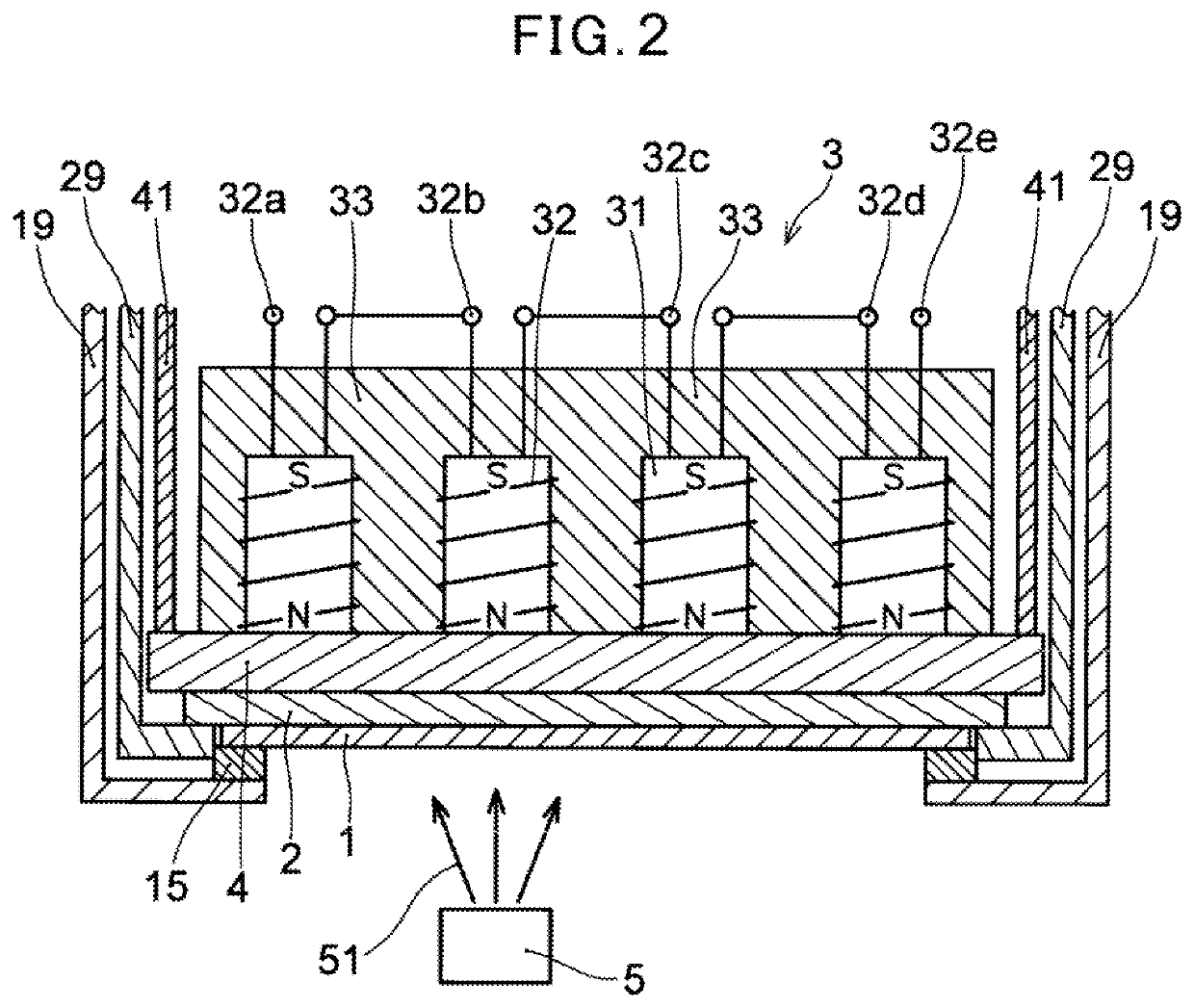
[0062]At the time of alignment between the vapor-deposition mask 1 and the substrate to be vapor-deposited 2 the vapor-deposition apparatus also comprises a micro-motion apparatus which relatively moves the substrate to be vapor-deposited 2 with respect to the vapor-deposition mask 1 while imaging an alignment mark formed on each of the vapor-deposition mask 1 and the substrate to be vapor-deposited 2. Alignment is carried out while stopping supplying power to the electromagnet 3 so that the vapor-deposition mask 1 is not unnecessarily suctioned by the electromagnet 3. Thereafter, the electromagnet 3 being held by a similar holder (not shown) or the touch plate 4 to be lowered to cause current to flow causes the vapor-deposition mask 1 to be suctioned toward the substrate to be vapor-deposited 2.
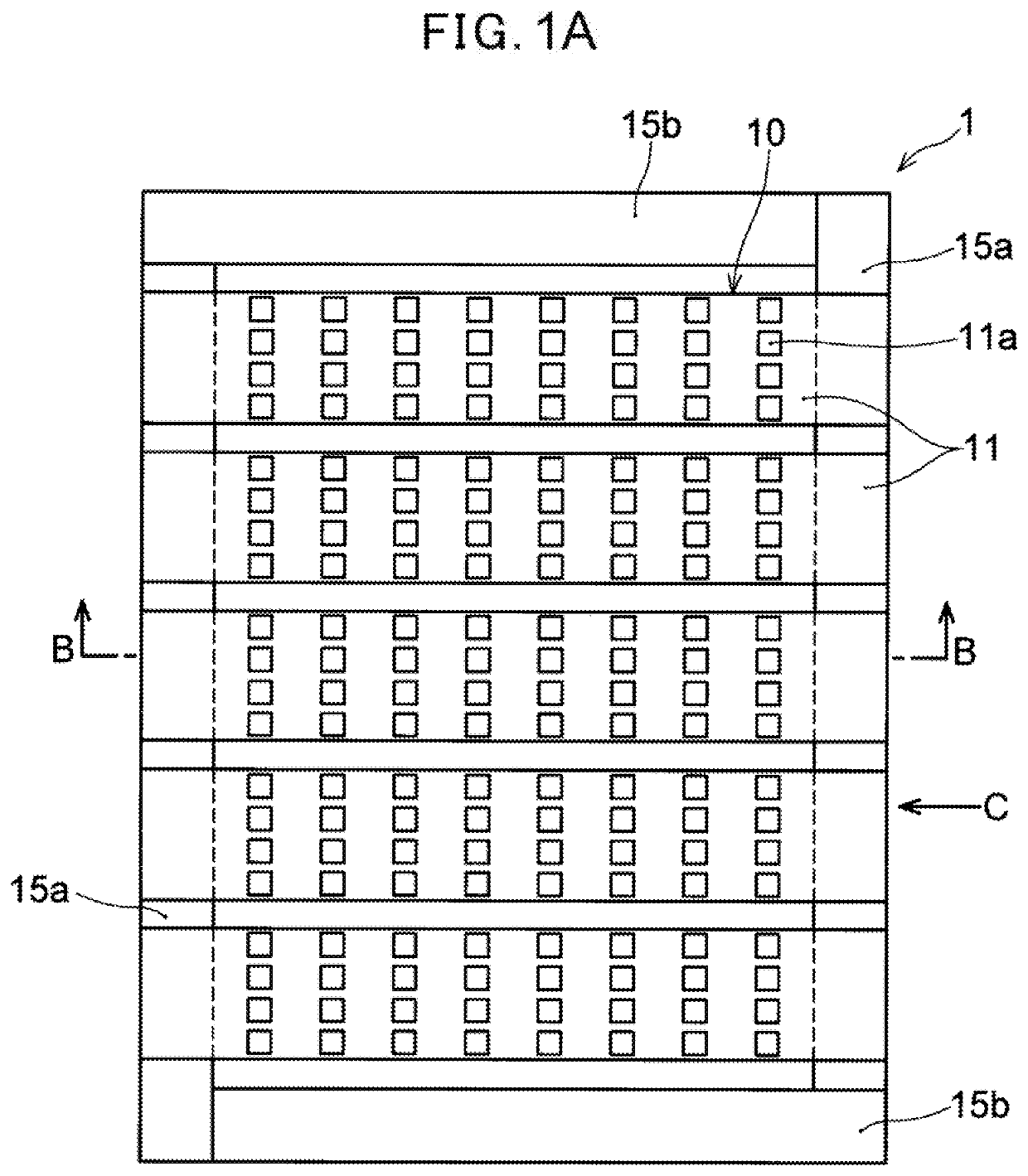
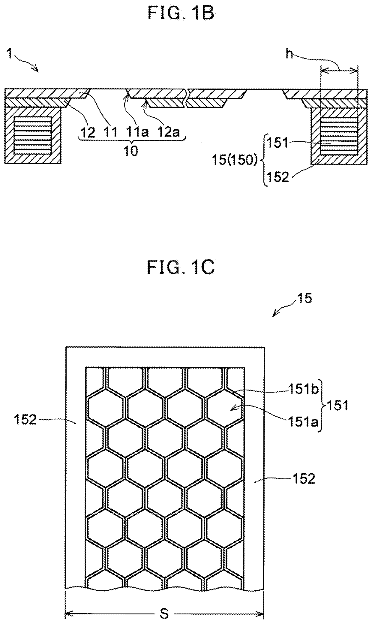
[0063]According to the present embodiment, a structure in which the core portion 151 of the sandwich structure 150 comprising a gap is sandwiched by the end plate 152 is used for the frame ...
third embodiment
[0072]A method for manufacturing an organic-EL display apparatus according to the present invention comprises: forming a TFT (not shown), a planarizing film, and a first electrode 22 (for example, an anode) on a supporting substrate 21;
[0073]overlapping a vapor-deposition mask 1 aligning to the first electrode 22 being oriented downward; and, in vapor-depositing a vapor-deposition material 51, forming a deposition layer 25 of an organic layer using the previously-described vapor-deposition method. In this way, a second electrode 26 (see FIG. 7B; a cathode) is formed on the deposition layer 25.
[0074]While the supporting substrate 21 such as a glass plate, for example, is not shown fully, a driving element such as a TFT is formed. for a RGB sub-pixel of each pixel, and the first electrode 22 that is connected to the above-mentioned driving element is formed on the planarizing layer by a combination of an ITO layer and a layer of metal such as Ag or APC. As shown in FIGS. 7A and 7B, an...
second embodiment
[0089](10) Moreover, a method of vapor deposition according to the present invention comprises: arranging a substrate to be vapor-deposited and the vapor-deposition mask as described in one of (1) to (9) such that they overlap each other; and depositing the vapor-deposited material onto the substrate to be vapor-deposited by causing a vapor-deposited material to fly away from a vapor-deposition source arranged at a distance from the vapor-deposition mask.
[0090]The vapor-deposition method according to the second embodiment of the present invention makes it easier to handle the vapor-deposition mask with a robot arm since the vapor-deposition mask is made very lightweight, and a further upsizing of the substrate is realized.
[0091](11) The frame of the vapor-deposition mask having a frame-like rectangular shape and the substrate to be vapor-deposited and the vapor-deposition mask being arranged such that a side of the frame formed such that the gap faces the outside of the frame from t...
PUM
| Property | Measurement | Unit |
|---|---|---|
| Shape | aaaaa | aaaaa |
| Distance | aaaaa | aaaaa |
Abstract
Description
Claims
Application Information
 - R&D
- Intellectual Property
- Life Sciences
- Materials
- Tech Scout
- Unparalleled Data Quality
- Higher Quality Content
- 60% Fewer Hallucinations
Browse by: Latest US Patents, China's latest patents, Technical Efficacy Thesaurus, Application Domain, Technology Topic, Popular Technical Reports.
© 2025 PatSnap. All rights reserved.Legal|Privacy policy|Modern Slavery Act Transparency Statement|Sitemap|About US| Contact US: help@patsnap.com