Electronic device including display module including sensor and method for manufacturing the display module

Active Publication Date: 2020-08-20
SAMSUNG ELECTRONICS CO LTD
View PDF0 Cites 3 Cited by
  • Summary
  • Abstract
  • Description
  • Claims
  • Application Information

AI Technical Summary

Benefits of technology

The patent text describes an adhesive material used to bond a display module and a sensor in an electronic device. The adhesive material has specific mechanical and thermal characteristics, including a glass transition temperature and a modulus of elasticity. By adjusting these characteristics, the adhesive material can alleviate internal or external stress during the bonding process and improve signal transmission performance in the ultrasonic band. The patent also describes different preparation examples of the adhesive material using different compounds. The technical effect of this patent is to improve the bonding process in electronic devices and improve the performance of the sensor.

Problems solved by technology

The adhesive film may not ensure mechanical reliability for a drop impact.
Furthermore, the attachment structure including the adhesive film may deteriorate the performance (e.g., the signal to noise ratio (SNR)) of the sensor because the ultrasonic impedance of an adhesive material is relatively very low, compared with that of the display or the sensor.

Method used


Image

  • Electronic device including display module including sensor and method for manufacturing the display module
  • Electronic device including display module including sensor and method for manufacturing the display module
  • Electronic device including display module including sensor and method for manufacturing the display module

Examples


Embodiment Construction

[0022]Hereinafter, various embodiments of the disclosure will be described with reference to the accompanying drawings. However, those of ordinary skill in the art will recognize that modification, equivalent, and / or alternative on the various embodiments described herein can be variously made without departing from the scope and spirit of the disclosure.

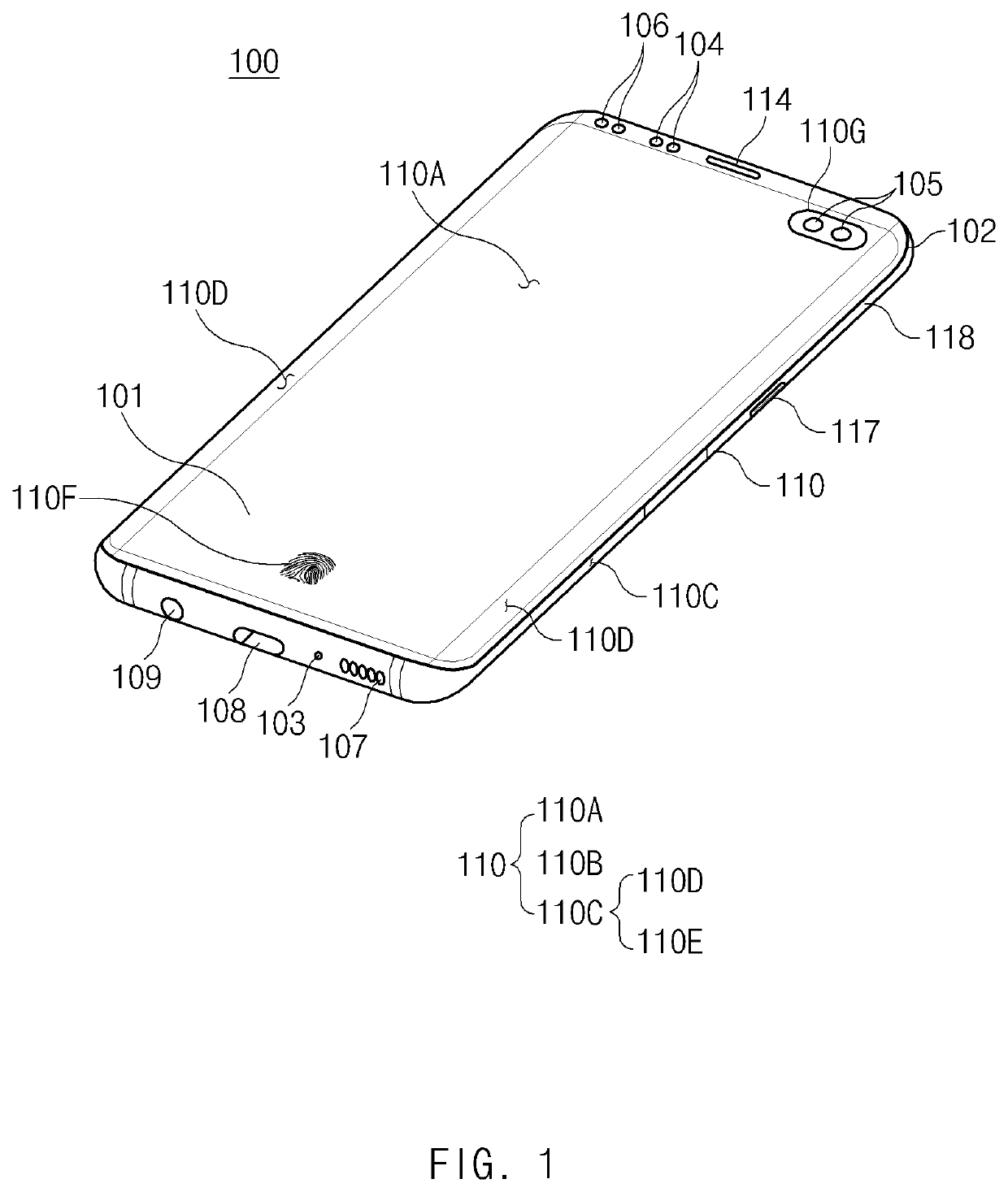
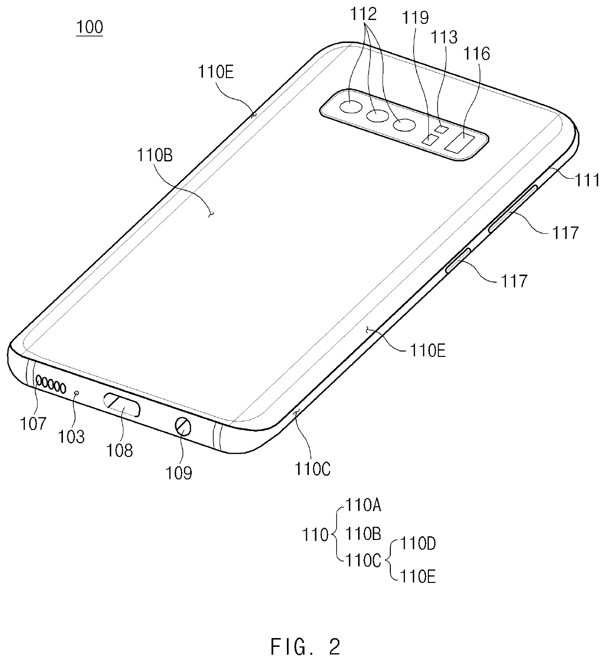
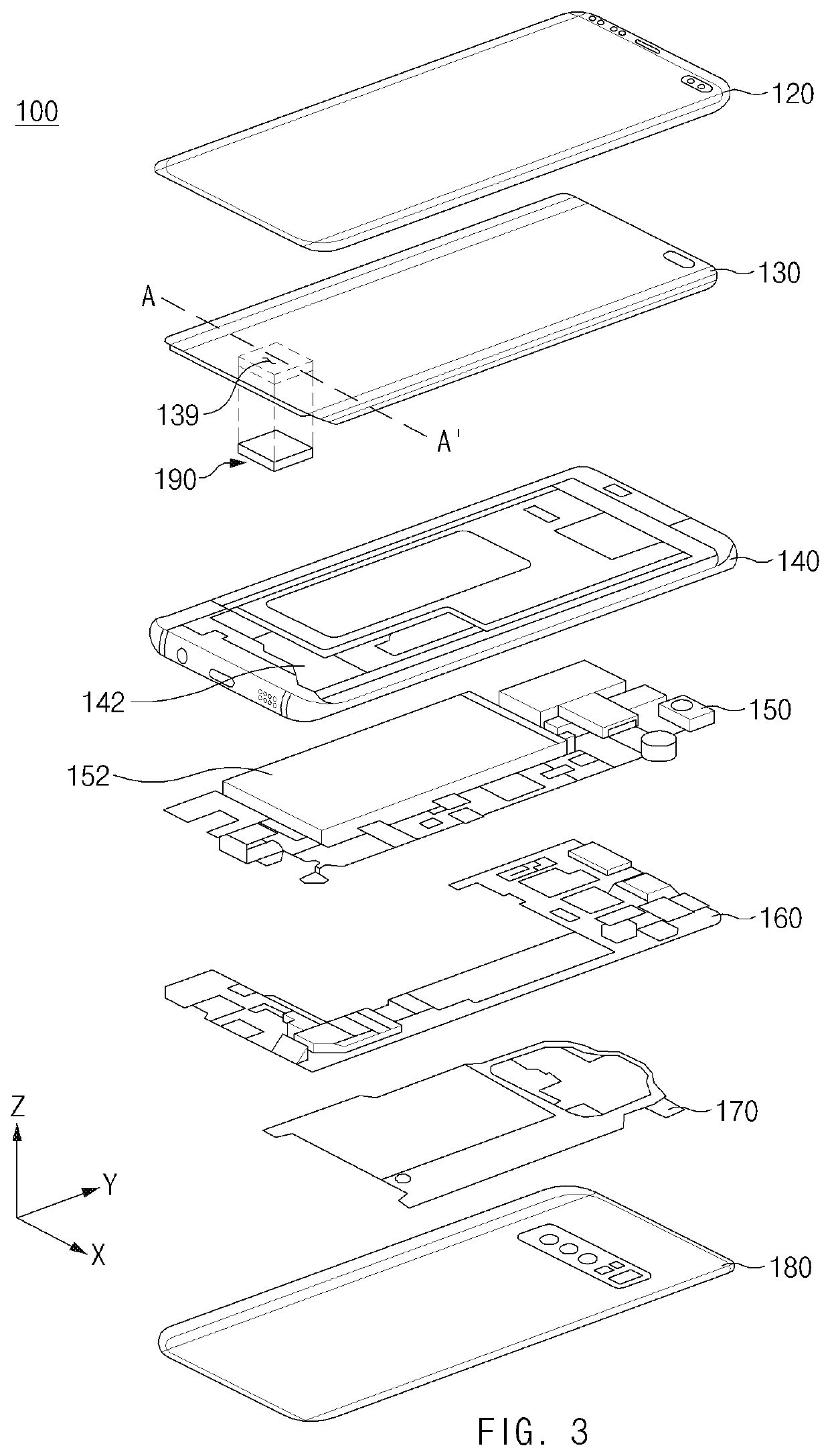
[0023]FIG. 1 is a front perspective view of an electronic device according to an embodiment. FIG. 2 is a rear perspective view of the electronic device illustrated in FIG. 1.

[0024]Referring to FIGS. 1 and 2, the electronic device 100 may include a housing 110 that includes a first surface (or a front surface) 110A, a second surface (or a rear surface) 110B, and side surfaces 110C that surround a space between the first surface 110A and the second surface 110B.

[0025]In another embodiment, the housing 110 may refer to a structure that forms some of the first surface 110A, the second surface 110B, and the side surfaces 110C of FIG. 1.

[...


PUM


Abstract

Disclosed is an electronic device that includes a housing, a display module that includes a first panel including a first surface, a second surface opposite to the first surface, and a plurality of pixels disposed between the first surface and the second surface, a cover layer that is disposed on the first surface of the first panel and that forms one surface of the housing, and a second panel disposed on the second surface of the first panel, and a sensor that is coupled to the display module and that forms a sensing area on the one surface of the housing. The display module includes an opening that is formed through the second panel and in which the sensor is disposed, and the sensor includes an active area and an inactive area formed around the active area. A first adhesive material is formed between the active area and the first panel. The first adhesive material includes a mechanical or thermal characteristic that a glass transition temperature Tg ranges from 0° C. to 25° C. in a frequency condition of 0.01 Hz to 0.1 Hz, a modulus of elasticity at 35° C. or more is 0.2 GPa or less, and a modulus of elasticity at −10° C. or less is 1 GPa or more.

Description

CROSS-REFERENCE TO RELATED APPLICATION(S)[0001]This application is based on and claims priority under 35 U.S.C. § 119 to Korean Patent Application No. 10-2019-0019472, filed on Feb. 19, 2019, and Korean Patent Application No. 10-2019-0018070, filed on Feb. 15, 2019, in the Korean Intellectual Property Office, the disclosures of each of which are incorporated by reference herein in their entireties.BACKGROUND1. Field[0002]The disclosure relates generally to an electronic device having a display module including a sensor and a method for manufacturing the display module, and more particularly, to an electronic device having a display module including a sensor that forms a sensing area that overlaps a screen display area.2. Description of the Related Art[0003]An electronic device may include a sensor that provides a fingerprint recognition function, which may be disposed on a lower side of a display area on the exterior of the electronic device, or may be disposed on a rear case of the...

Claims


Application Information

Patent Timeline
IPC IPC(8): G06K9/00H04M1/02
CPCG06K9/0002H04M1/0266H04M1/026H04M2250/12G06V40/1306
Inventor LEE, YONGWONKIM, IIKANG, DAREUMPARK, CHOHEEBAE, DOHYUNJEONG, HYEONCHEOLJO, JEONGGYUCHOI, SEONGWOORHEE, BONGJAE
Owner SAMSUNG ELECTRONICS CO LTD
Why Eureka
Try Eureka