
Interface circuit and communication apparatus

a communication apparatus and interface circuit technology, applied in the direction of amplifiers, amplifier types, amplifiers with semiconductor devices/discharge tubes, etc., can solve the problems of increased circuit scale and increased power consumption, and achieve the effect of reducing circuit scale and power consumption of the communication apparatus and reducing circuit scale and power consumption

Active Publication Date: 2020-06-18
MURATA MFG CO LTD
View PDF0 Cites 0 Cited by
  • Summary
  • Abstract
  • Description
  • Claims
  • Application Information

AI Technical Summary

Benefits of technology

The present disclosure provides an interface circuit and a communication apparatus that can reduce the circuit size and power consumption. By sharing the use of the AD conversion circuit, multiple communication devices can work together, reducing the overall size and power consumption of the circuit. This results in a more efficient and compact communication apparatus.

Problems solved by technology

In a configuration that includes, for example, communication devices for a wireless LAN and for LTE communication, if a temperature sensor and an analog-to-digital (AD) conversion circuit are disposed for each communication device, an issue of increased circuit scale and increased power consumption arises.

Method used


Image

  • Interface circuit and communication apparatus
  • Interface circuit and communication apparatus
  • Interface circuit and communication apparatus

Examples


first embodiment

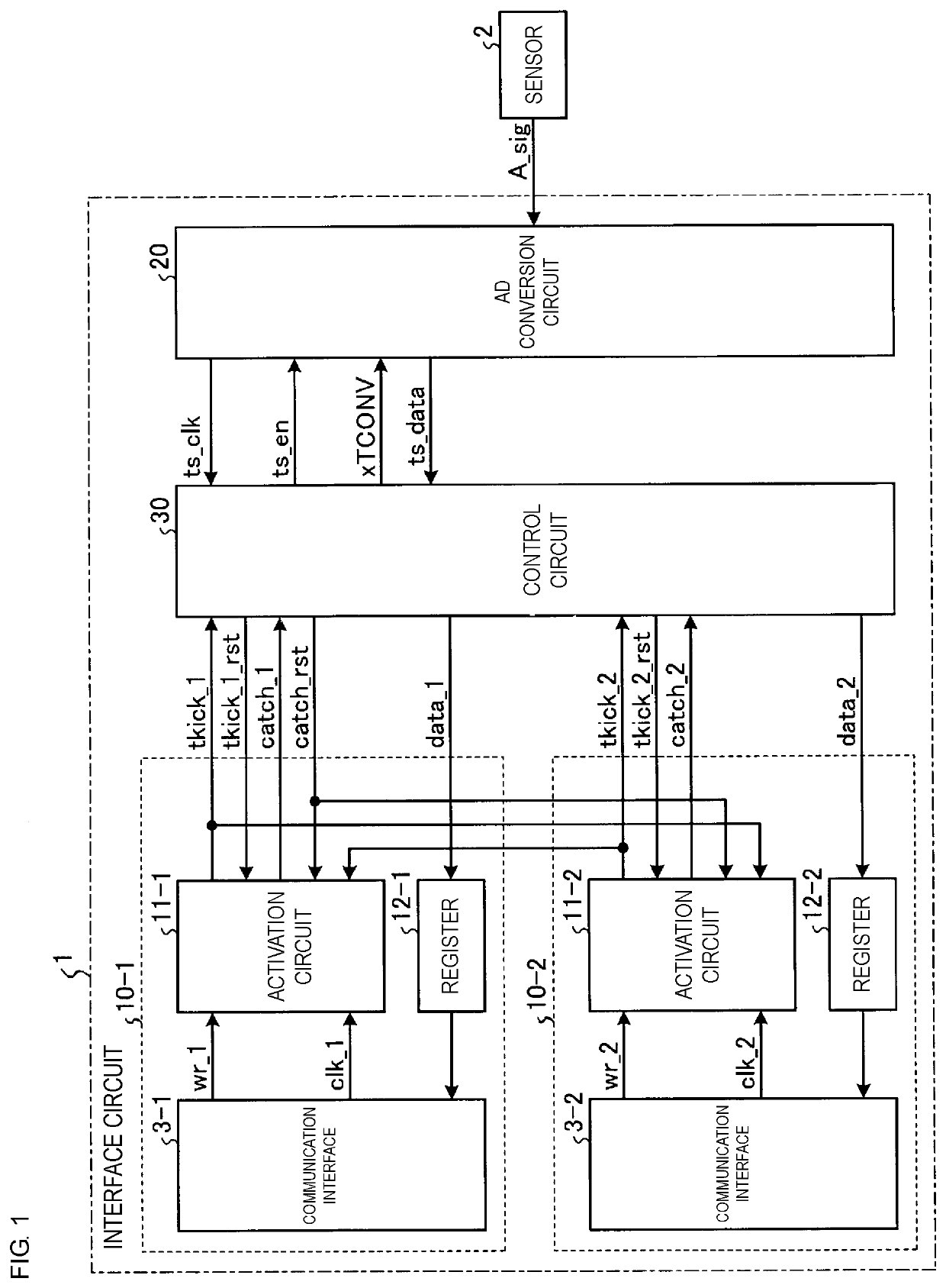
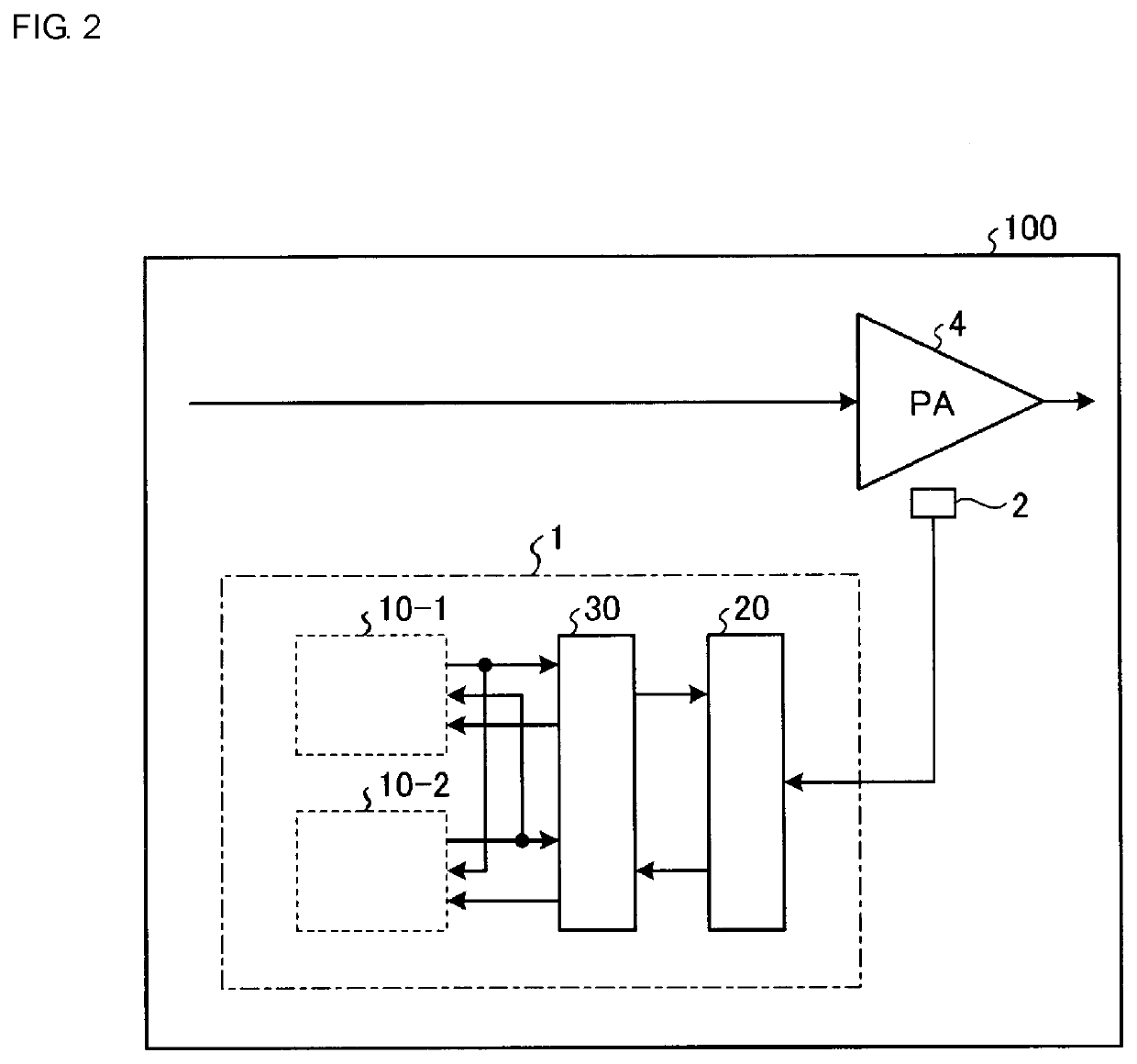
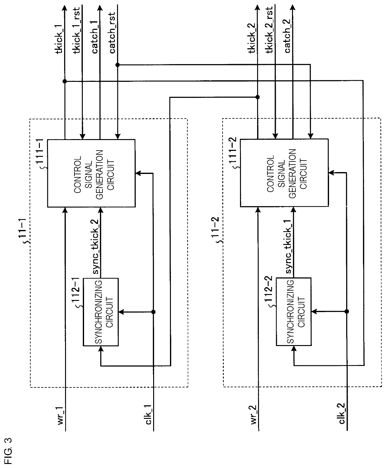
[0032]FIG. 1 is a block diagram depicting an example of a schematic configuration of an interface circuit according to an embodiment. FIG. 2 depicts an example of major components of a communication apparatus according to the embodiment. As depicted in FIG. 1, an interface circuit 1 includes communication devices 10-1 and 10-2, an analog-to-digital (AD) conversion circuit 20, and a control circuit 30. In this disclosure, the communication device 10-1 is, for example, a communication device used for 5 GHz band Long Term Evolution (LTE) communication, and the communication device 10-2 is, for example, a communication device for Wi-Fi communication. In this disclosure, the AD conversion circuit 20 converts an analog signal A_sig received from a sensor 2 to digital data ts_data. In the configuration according to this disclosure, the two communication devices 10-1 and 10-2 share the use of the sensor 2 and the AD conversion circuit 20. In the following description, the two communication ...

second embodiment

[0084]FIG. 17 depicts an example configuration in which six communication devices share the use of the AD conversion circuit 20. FIG. 18 depicts example destinations to which the digital data ts_data is output in the example configuration depicted in FIG. 17.

[0085]In the example configuration depicted in FIG. 17, as depicted in EXAMPLE 1 in FIG. 18, if an activation signal tkick_1 is output from a communication device 10-1 and afterward a capture signal catch_5 is output from a communication device 10-5 during the waiting period P1, the control circuit 30 sets the communication device 10-1 and the communication device 10-5 as destinations to which the digital data ts_data is output.

[0086]In the example configuration depicted in FIG. 17, as depicted in EXAMPLE 2 in FIG. 18, if an activation signal tkick_4 is output from a communication device 10-4 and afterward a capture signal catch_1 is output from the communication device 10-1 and a capture signal catch_6 is output from a communic...


PUM


Abstract

An interface circuit and a communication apparatus that can reduce the circuit scale and power consumption are provided. An interface circuit includes a plurality of communication devices, an analog-to-digital (AD) conversion circuit that converts an analog signal to digital data, and a control circuit that reads the digital data in response to read-request signals received from the plurality of communication devices.

Description

[0001]This application claims priority from Japanese Patent Application No. 2018-233833 filed on Dec. 13, 2018 and Japanese Patent Application No. 2019-170793 filed on Sep. 19, 2019. The content of these applications are incorporated herein by reference in their entireties.BACKGROUND[0002]The present disclosure relates to an interface circuit and a communication apparatus.[0003]Recent mobile communication terminals, such as cellular phones and smartphones, are required to achieve multiband or multimode communication, in which a single terminal is capable of communicating by using a plurality of frequencies or a plurality of wireless communication schemes. Such communication apparatuses as are capable of multiband or multimode communication are required to process a plurality of transmit / receive signals at high speed without necessarily degrading quality. For example, Licensed-Assisted Access (LAA) has been standardized. This technology uses the unlicensed 5 GHz band, which is used f...

Claims


Application Information

Patent Timeline
Patent Type & Authority Applications(United States)
IPC IPC(8): H04B1/00H03F3/195
CPCH03F2200/451H04B1/0007H03F3/195H04B1/04H04B2001/0408
Inventor MATSUMURA, TOSHIKISHINTOMI, YUJIMATSUMURA, SATOSHINAKAMUTA, KAZUHIRO
Owner MURATA MFG CO LTD
Learn More