Chip package circuit board module

a technology of circuit board and chip, applied in the field of circuit board modules, can solve the problems of low reliability of circuit board, reduced yield, and packaging new led chips at the same position, and achieve the effects of high yield rate, rapid and easy disposal of circuit board, and intensive and flexible design

Active Publication Date: 2018-12-20
UNIMICRON TECH CORP
View PDF1 Cites 0 Cited by
  • Summary
  • Abstract
  • Description
  • Claims
  • Application Information

AI Technical Summary

Benefits of technology

[0004]The invention provides a chip package circuit board module, which has a substitute chip that can be rapidly and easily disposed on a circuit board, a high yield rate, and a more intensive and more flexible design for routing on a surface while allowing the surface to include less glossy for reducing influences on display presentation.
[0016]Based on the above, according to the chip package circuit board module of the invention, the first pad, the second pad and the substitute pad for the second pad are disposed on the circuit board and separated from one another. Also, the first pad has the portion corresponding to the second pad and the portion corresponding to the substitute pad, and the original chip is connected to the first pad and the second pad. When the original chip is inoperative, the substitute chip can be directly connected to the first pad and the substitute pad, and connected to the substitute pad and the second pad through the additionally-disposed conductive member. Accordingly, it is not required to remove the original chip during the reworking process but directly replace the original chip with the substitute chip, and thus the steps in the reworking process can be effectively reduced. Alternatively, the chip package circuit board module of the invention can adopt the multi-layer circuit board in which the second pad and the substitute pad for the second pad are connected through in the inner layer in advance. In this way, when the original chip is inoperative, the substitute chip can operate as a replacement of the original chip simply by directly connecting the substitute chip to the first pad and the substitute pad without removing the original chip.

Problems solved by technology

However, when the LED chip is unable to emit light due to damages, packaging failures or other reasons, it is required to remove the LED chip, and clean up pads on the circuit board (sometimes, reprinting solder paste is also required) before a new LED chip can be packaged again.
Nonetheless, a reworking process as described above may face the following problems: copper wires on a surface of the circuit board may be peeled off together when the LED chip is to be peeled off; because it may require a high temperature to applied in the process of peeling off the LED chip, the circuit board may exhibit unexpected thermal expansion or contraction in the high temperature environment which may damage the circuit board and lower a reliability of the circuit board; since the pads may be damaged when the LED chip is to be peeled off, packaging the new LED chip at the same position may face issues like yield reduction.

Method used


Image

  • Chip package circuit board module
  • Chip package circuit board module
  • Chip package circuit board module

Examples


Embodiment Construction

[0029]Reference will now be made in detail to the present preferred embodiments of the invention, examples of which are illustrated in the accompanying drawings. Wherever possible, the same reference numbers are used in the drawings and the description to refer to the same or like parts.

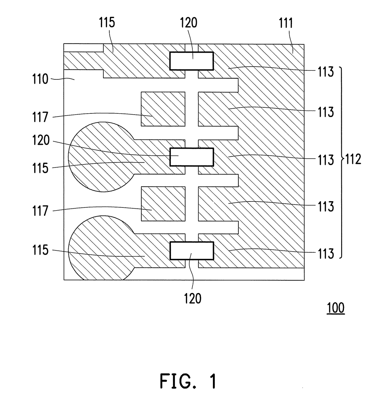
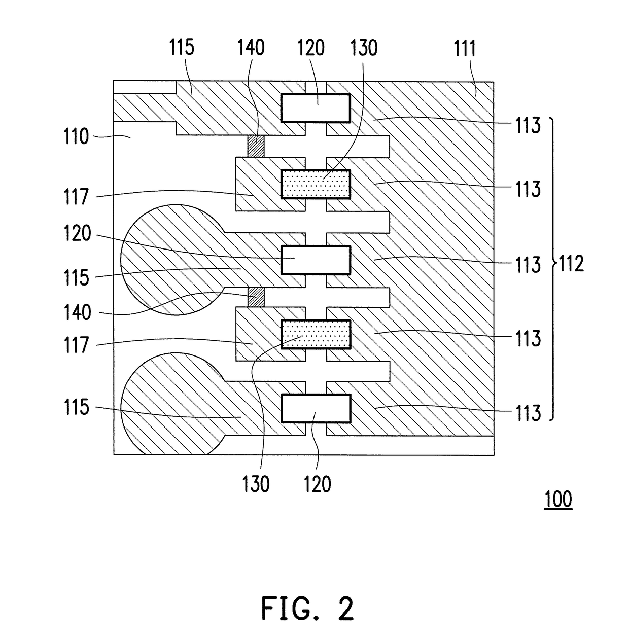
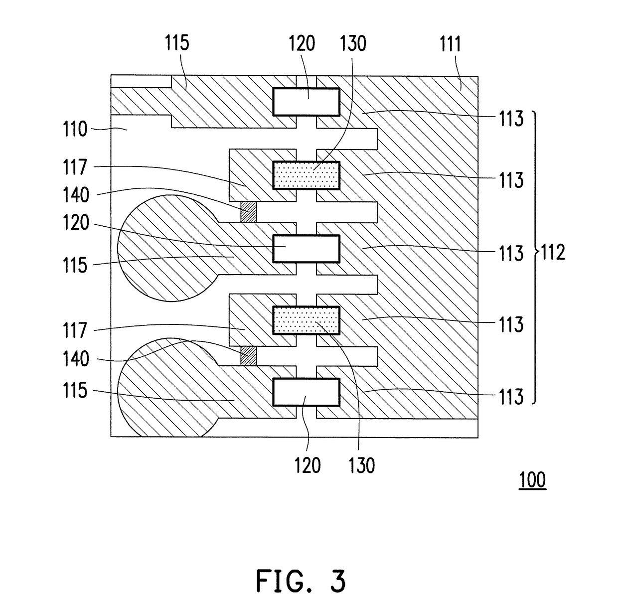
[0030]FIG. 1 is a schematic diagram of a chip package circuit board module according to an embodiment of the invention. With reference to FIG. 1, a chip package circuit board module 100 of the present embodiment includes a circuit board 110 and at least one original chip 120. The circuit board 110 includes at least one first pad 112, at least one second pad 115 and at least one substitute pad 117. In the present embodiment, the first pad 112 includes at least one first branch 113, and these first branches 113 are connected to one another and correspond to the second pad 115 and the substitute pad 117, respectively. In view of FIG. 1, the first branches 113 of the first pad 112 are connected through a...


PUM


Abstract

A chip package circuit board module including a circuit board and at least one original chip is provided. The circuit board includes at least one first pad, at least one second pad and at least one substitute pad. The at least one second pad is located besides the at least one first pad and separated from the at least one first pad. The at least one substitute pad is adjacent to the at least one second pad and separated from the at least one first pad and the at least one second pad. The at least one original chip is connected to the at least one first pad and at least one the second pad, respectively. A total width of a portion corresponding to each of the at least one second pad and a portion corresponding to the substitute pad adjacent to the second pad of the first pad is greater than or equal to twice a width of the original chip.

Description

BACKGROUND OF THE INVENTION1. Field of the Invention[0001]The invention relates to a circuit board module, and more particularly, to a chip package circuit board module.2. Description of Related Art[0002]In general, a circuit board module of a light-emitting diode (LED) chip has a LED chip packaged onto a circuit board. However, when the LED chip is unable to emit light due to damages, packaging failures or other reasons, it is required to remove the LED chip, and clean up pads on the circuit board (sometimes, reprinting solder paste is also required) before a new LED chip can be packaged again.[0003]Nonetheless, a reworking process as described above may face the following problems: copper wires on a surface of the circuit board may be peeled off together when the LED chip is to be peeled off; because it may require a high temperature to applied in the process of peeling off the LED chip, the circuit board may exhibit unexpected thermal expansion or contraction in the high temperat...

Claims


Application Information

Patent Timeline
Patent Type & Authority Applications(United States)
IPC IPC(8): H05K1/18H05K1/11
CPCH05K1/181H05K1/111H05K1/0292H05K1/0295H05K3/225H05K2201/10106
Inventor LIU, WEN-FANGLEE, SHAO-CHIENTSENG, CHEN-WEILI, ZONG-HUALI, CHIEN-TSAI
Owner UNIMICRON TECH CORP
Why Eureka
Try Eureka