In-Vehicle Semiconductor Device
a semiconductor device and vehicle technology, applied in the direction of pulse technique, electric control, instruments, etc., can solve the problems of extremely fast frequency supply, the regulator cannot supply a rated internal voltage, etc., and achieve the effect of high resistance against malfunction
- Summary
- Abstract
- Description
- Claims
- Application Information
AI Technical Summary
Benefits of technology
Problems solved by technology
Method used
Image
Examples
first embodiment
[0050]An embodiment will now be described in detail.
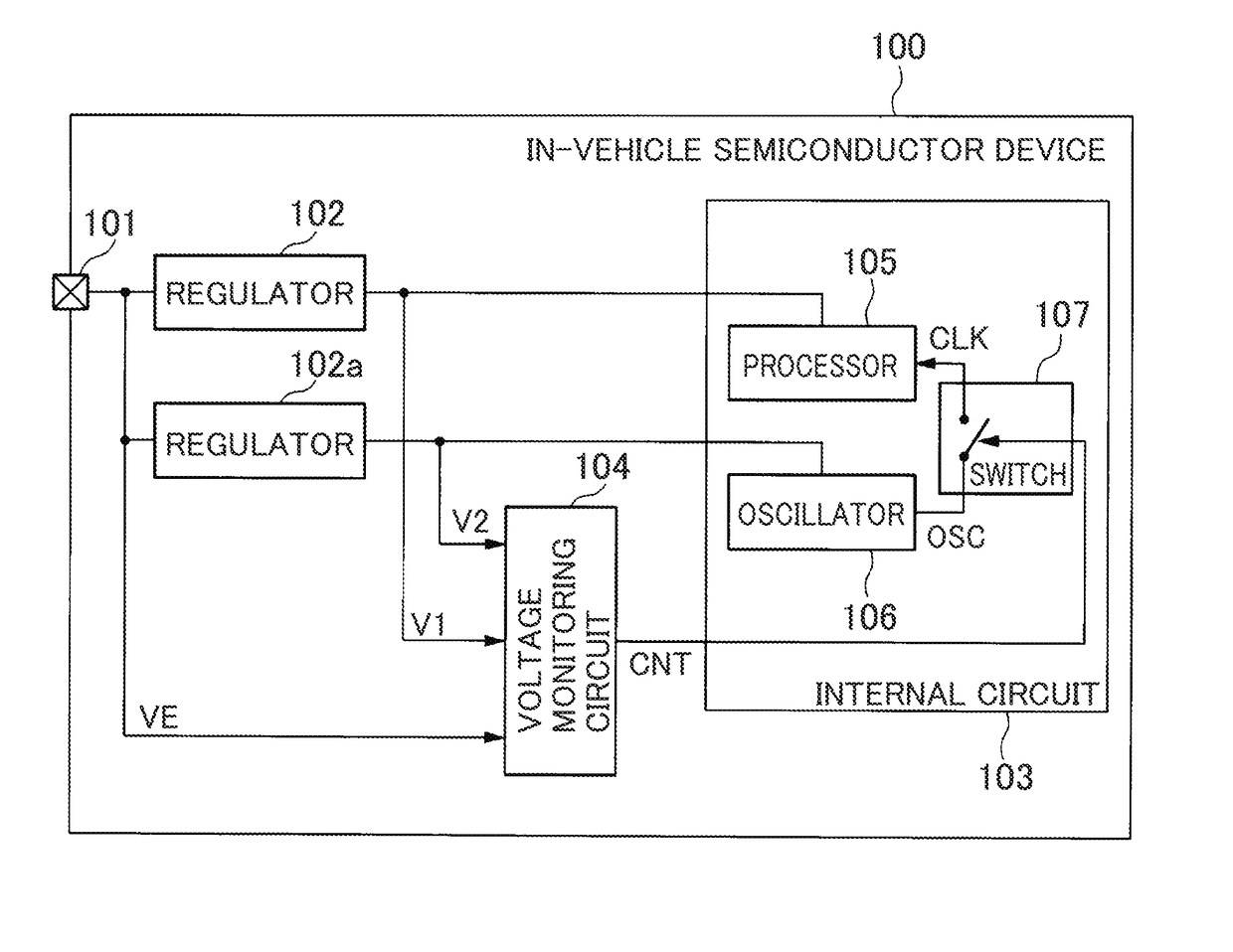
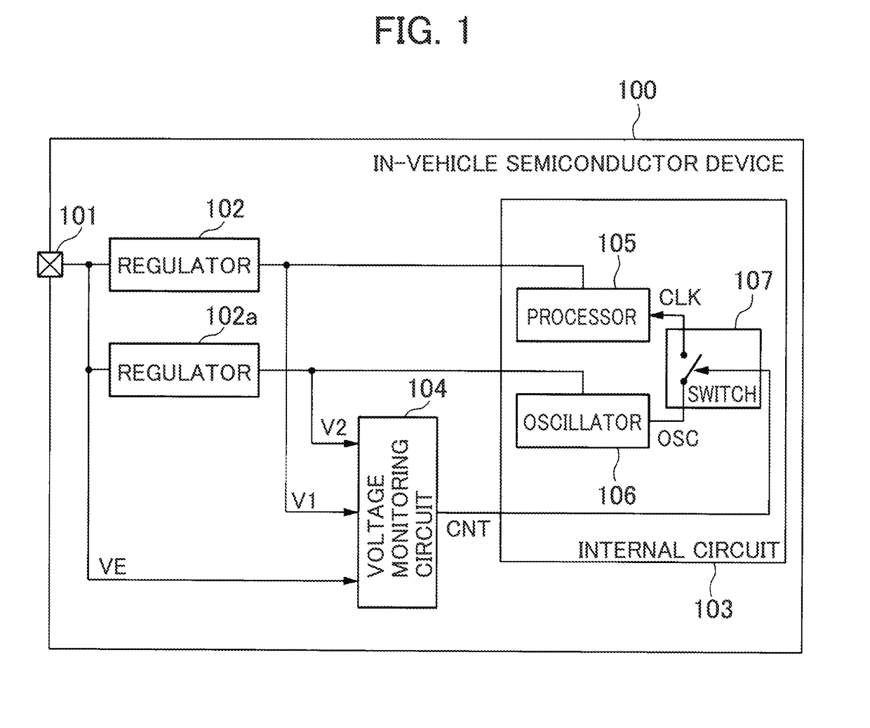
[0051]FIG. 1 is an illustrative block diagram showing an example configuration of an in-vehicle semiconductor device 100 in accordance with a first embodiment.
[0052]As illustrated in FIG. 1, the in-vehicle semiconductor device 100 has a power supply terminal 101, regulators 102, 102a, an internal circuit 103, and a voltage monitoring circuit 104. The power supply terminal 101 is an external input terminal to which a voltage VE which is operation voltage of the in-vehicle semiconductor device 100 is supplied.
[0053]The voltage VE is a first voltage, for example, a voltage of around 5 V. The voltage VE is supplied from, for example, an ECU which is not shown. The ECU is a unit that acquires information from, for example, each of sensors of an engine power train, and calculates a most-suitable amount of fuel injection, most-suitable fuel-injection timing, most-suitable ignition timing, a most-suitable idling speed, and the like for the...
second embodiment
[0097]In a second embodiment, a technique is described by which the reliability of the voltage monitoring circuit 104 can be increased by decreasing a drop in the voltage VM serving as an operation voltage of the voltage monitoring circuit 104 itself, during the application of surge.
[0098]FIG. 5 is an illustrative block diagram showing an example configuration of the in-vehicle semiconductor device 100 in accordance with the second embodiment.
[0099]The in-vehicle semiconductor device 100 illustrated in FIG. 5 further includes a regulator 500, a capacitor 501 and a level conversion circuit 502 in addition to a configuration similar to the configuration illustrated in FIG. 1 in accordance with the first embodiment in which the power supply terminal 101, the regulators 102, 102a, the internal circuit 103 and the voltage monitoring circuit 104 are included.
[0100]The regulator 500 is a third regulator, which generates a voltage VM from the voltage VE supplied from the ECU. The voltage VM...
third embodiment
[0105]In the third embodiment, a technique is described by which to lessen the voltage drop in the voltages V1, V2 to be provided to the internal circuit 103 of the in-vehicle semiconductor device 100.
[0106]FIG. 6 is an illustrative block diagram showing an example configuration of the in-vehicle semiconductor device 100 in accordance with the third embodiment.
[0107]The in-vehicle semiconductor device 100 illustrated in FIG. 6 further includes a surge protection circuit 600 and a backup circuit 601 in addition to a configuration similar to the in-vehicle semiconductor device 100 illustrated in FIG. 1 in accordance with the first embodiment. Other connection arrangements are similar to FIG. 1, and a description is omitted.
[0108]The surge protection circuit 600 has a surge protection resistor 602 and a clamping element 603. The surge protection resistor 602 is a resistor and the clamping element 603 is a diode.
[0109]The surge protection circuit 600 is a circuit to protect the regulato...
PUM
 Abstract
Description
Claims
Application Information
 - R&D Engineer
- R&D Manager
- IP Professional
- Industry Leading Data Capabilities
- Powerful AI technology
- Patent DNA Extraction
Browse by: Latest US Patents, China's latest patents, Technical Efficacy Thesaurus, Application Domain, Technology Topic, Popular Technical Reports.
© 2024 PatSnap. All rights reserved.Legal|Privacy policy|Modern Slavery Act Transparency Statement|Sitemap|About US| Contact US: help@patsnap.com


