
Methods and apparatuses for etch profile optimization by reflectance spectra matching and surface kinetic model optimization

a technology of reflectance spectra and optimization methods, applied in the direction of photomechanical equipment, instruments, originals for photomechanical treatment, etc., can solve the problems of insufficient automation of procedures, insufficient and inability to achieve the degree of accuracy and reliability to find substantial use in the semiconductor processing industry

Active Publication Date: 2018-09-13
LAM RES CORP
View PDF0 Cites 10 Cited by
  • Summary
  • Abstract
  • Description
  • Claims
  • Application Information

AI Technical Summary

Benefits of technology

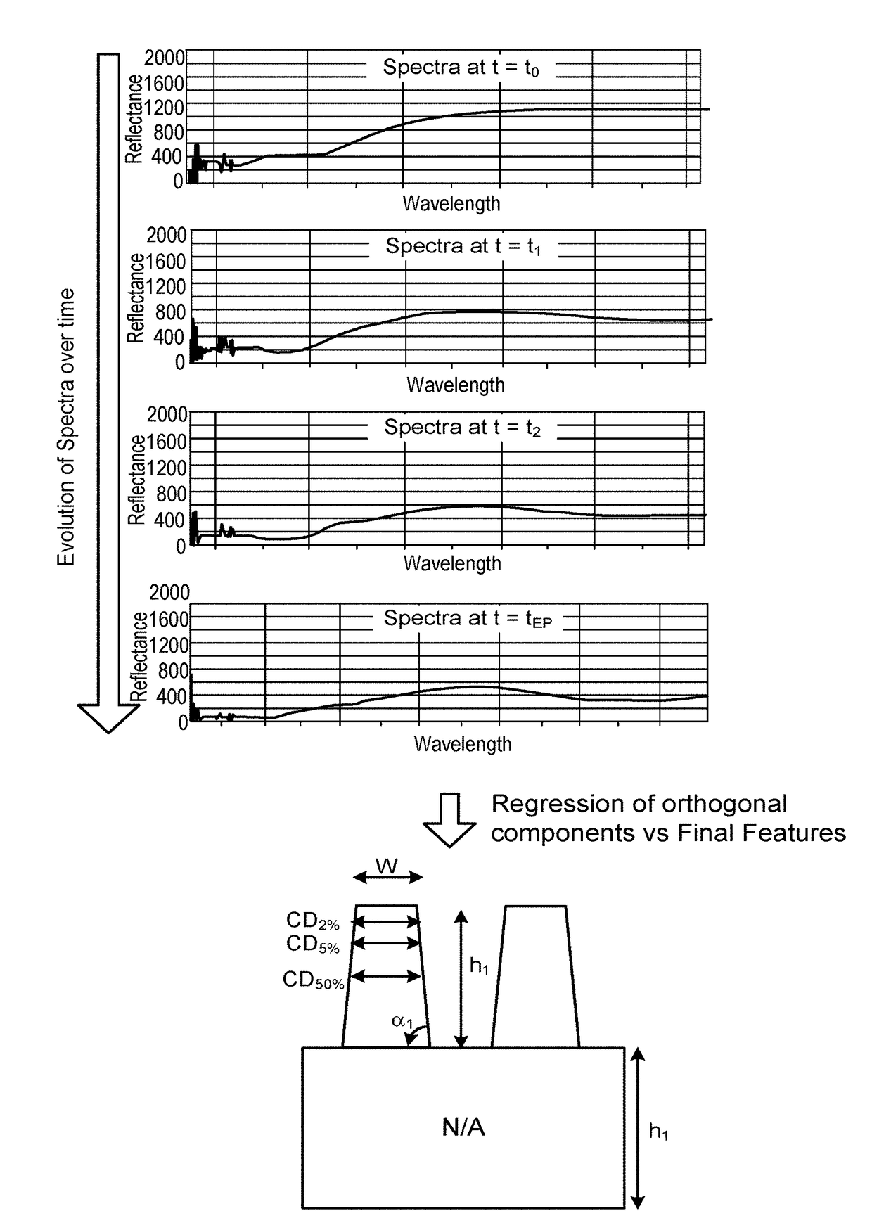
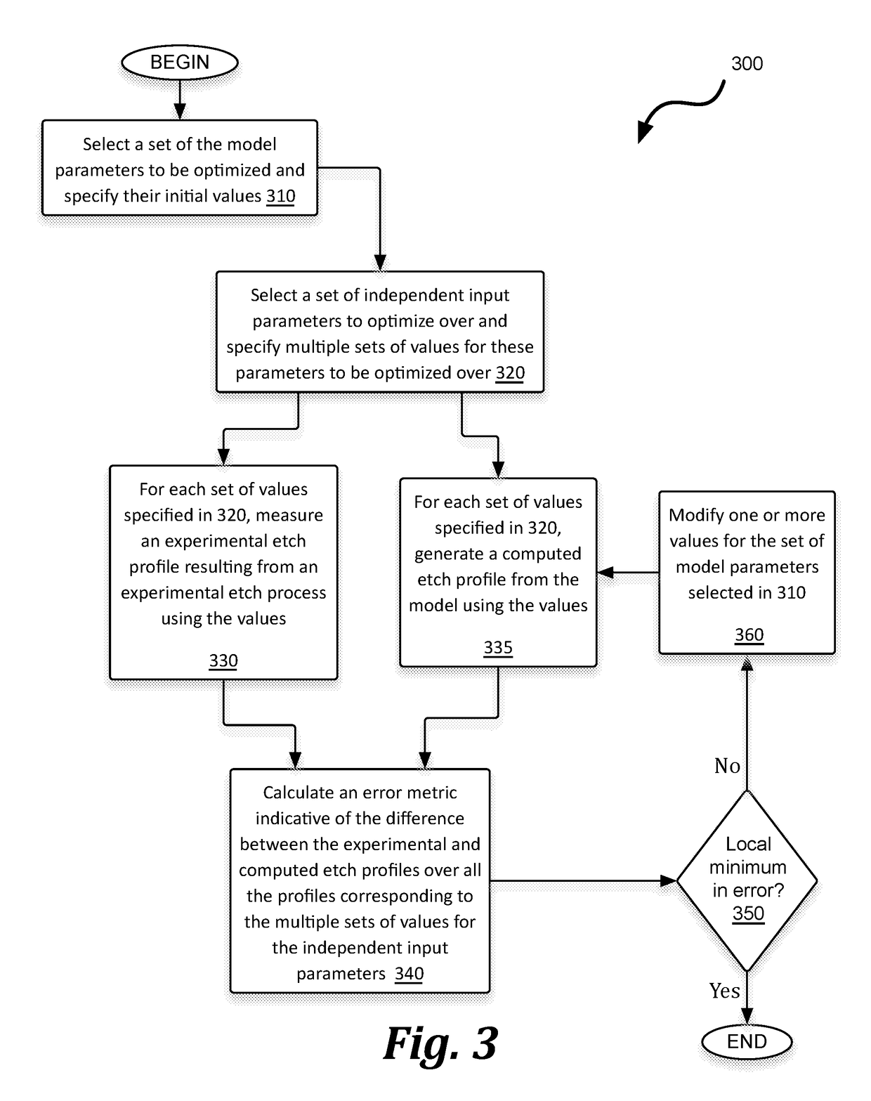
The patent describes methods and computer models for optimizing the etch process of a feature on a semiconductor substrate. These methods involve identifying a set of values for independent input parameters and using a plurality of model parameters to compute a reflectance spectra for the etch process. The methods also involve comparing the computed reflectance spectra to experimental reflectance spectra and modifying the model parameters to reduce the differences between them. The patent also discusses systems for processing semiconductor substrates with an etcher apparatus and a controller for adjusting its operation. The optimized etched feature profile model computed from the set of values for the independent input parameters can be used to compute the etched feature profile from a set of values for the input parameters. The technical effects of the patent include improving the accuracy and efficiency of the etch process and reducing the time and cost of research and development.

Problems solved by technology

However, optimizing the etch processes can be difficult and time-consuming, oftentimes involving process engineers manually tweaking etch process parameters in an ad hoc fashion in attempt to generate the desired target feature profile.
There is currently simply no automated procedure of sufficient accuracy which may be relied upon by process engineers to determine the values of process parameters which will result in a given desired etch profile.
Despite the extensive work done to develop these models, they do not yet possess the desire degree of accuracy and reliability to find substantial use within the semiconductor processing industry.

Method used


Image

  • Methods and apparatuses for etch profile optimization by reflectance spectra matching and surface kinetic model optimization
  • Methods and apparatuses for etch profile optimization by reflectance spectra matching and surface kinetic model optimization
  • Methods and apparatuses for etch profile optimization by reflectance spectra matching and surface kinetic model optimization

Examples


Embodiment Construction

Introduction

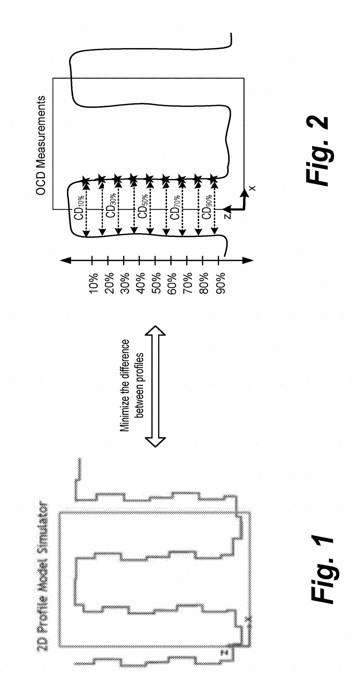
[0025]Disclosed herein are procedures for improving the practical utility of the etch profile models (EPMs) referred to above (and other similar models) so that they may be used to generate sufficiently accurate representations of semiconductor feature etch profiles, which are good enough approximations to be relied upon in the semiconductor processing industry. Generally, the inventive procedures improve these models' predictive power.

[0026]Generally, EPMs and similar models attempt to simulate the etch profile evolution of a substrate feature over time—i.e., the time-dependent changes in the shape of a feature at various spatial locations on the feature's surface—by calculating reaction rates associated with the etch process at each of these spatial locations which result from an incident flux of etchant and deposition species characteristic of the plasma conditions set up in the reaction chamber, and do so over the course of the simulated etch process. The output is a...


PUM


Abstract

Disclosed are methods of optimizing a computer model which relates the etch profile of a feature on a semiconductor substrate to a set of independent input parameters (A), via the use of a plurality of model parameters (B). In some embodiments, the methods may include modifying one or more values of B so as to reduce a metric indicative of the differences between computed reflectance spectra generated from the model and corresponding experimental reflectance spectra with respect to one or more sets of values of A. In some embodiments, calculating the metric may include an operation of projecting the computed and corresponding experimental reflectance spectra onto a reduced-dimensional subspace and calculating the difference between the reflectance spectra as projected onto the subspace. Also disclosed are etch systems implementing such optimized computer models.

Description

CROSS-REFERENCE TO RELATED APPLICATION[0001]This application is a continuation of U.S. patent application Ser. No. 15 / 698,458 filed Sep. 7, 2017, by Tetiker et al., entitled “METHODS AND APPARATUSES FOR ETCH PROFILE OPTIMIZATION BY REFLECTANCE SPECTRA MATCHING AND SURFACE KINETIC MODEL OPTIMIZATION, which is a continuation of U.S. patent application Ser. No. 15 / 018,708 filed on Feb. 8, 2016 (now U.S. Pat. No. 9,792,393), by Tetiker et al., entitled “METHODS AND APPARATUSES FOR ETCH PROFILE OPTIMIZATION BY REFLECTANCE SPECTRA MATCHING AND SURFACE KINETIC MODEL OPTIMIZATION,” which applications are incorporated by reference herein in their entirety and for all purposes.BACKGROUND[0002]The performance of plasma-assisted etch processes is frequently critical to the success of a semiconductor processing workflow. However, optimizing the etch processes can be difficult and time-consuming, oftentimes involving process engineers manually tweaking etch process parameters in an ad hoc fashion...

Claims


Application Information

Patent Timeline
IPC IPC(8): G06F17/50G03F7/00G01B11/00G01N21/55
CPCG06F17/5068G01N21/55G01B2210/56G01B11/002G03F7/00G06F17/5036G03F1/70G03F1/80G03F1/84G06F30/398H01L21/3065H01L21/31116H01L21/32136H01L21/67069G06F30/367G06F30/39
Inventor TETIKER, MEHMET DERYASRIRAMAN, SARAVANAPRIYANBAILEY, III, ANDREW D.PATERSON, ALEXGOTTSCHO, RICHARD A.
Owner LAM RES CORP
Learn More