
Electronic device using test pattern, method of analyzing test pattern, and non-transitory recording medium storing instructions to analyze test pattern

Active Publication Date: 2018-07-26
BROTHER KOGYO KK
View PDF0 Cites 1 Cited by
  • Summary
  • Abstract
  • Description
  • Claims
  • Application Information

AI Technical Summary

Benefits of technology

The patent text describes a method for forming test patterns on a sheet and analyzing them to determine control errors. The test patterns are formed quickly and accurately, and the control error can be determined with high accuracy based on the test patterns. The method involves acquiring image data of the test patterns and calculating the widths of the overlapping image of the test patterns at different positions in the reference direction. The test patterns include a model pattern and the widths of the overlapping image are compensated based on an error between the model pattern and the set width of the model pattern. The method allows for quick and accurate formation of test patterns and control error detection.

Problems solved by technology

According to the conventional technique, however, it is difficult to form the test patterns quickly (e.g., without minutely conveying the sheet), and determine the control error at high accuracy based on such test patterns.

Method used


Image

  • Electronic device using test pattern, method of analyzing test pattern, and non-transitory recording medium storing instructions to analyze test pattern
  • Electronic device using test pattern, method of analyzing test pattern, and non-transitory recording medium storing instructions to analyze test pattern
  • Electronic device using test pattern, method of analyzing test pattern, and non-transitory recording medium storing instructions to analyze test pattern

Examples


Embodiment Construction

[0036]Hereinafter, referring to the accompanying drawings, an illustrative embodiment according to the present disclosures will be described.

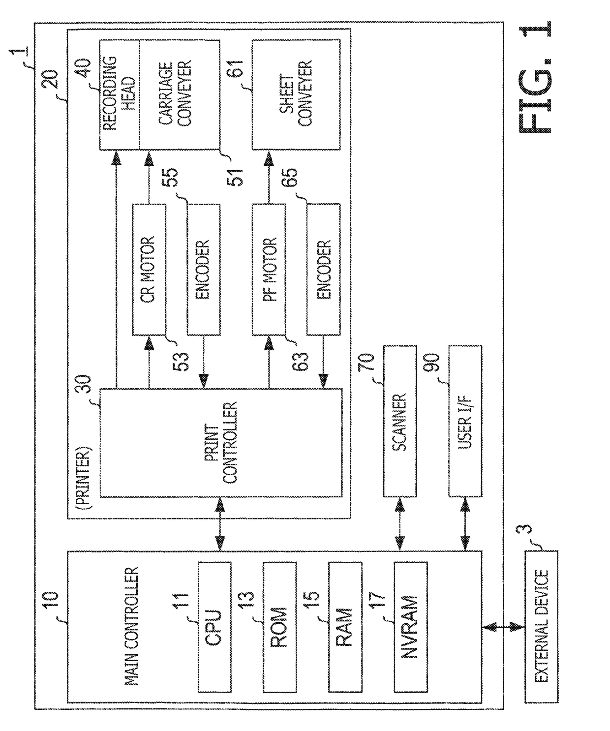
[0037]A digital MFP (hereinafter, simply referred to as MFP) 1 according to the illustrative embodiment of the present disclosures has, as shown in FIG. 1, a main controller 10, a printer 20, a scanner 70 and a user I / F 90. The main controller 10 controls an entire operation of the MFP 1 to make the MFP 1 function as a printing device, a scanning device and a copying device. The main controller 10 includes a CPU 11, a ROM 13, a RAM 15 and an NVRAM 17.

[0038]The CPU 11 executes processes in accordance with programs stored in the ROM 13 to realize the above functions. The RAM 15 is used as a work area when the CPU 11 executes the programs. The NVRAM 17 is an electrically rewritable non-volatile memory, and configured by a flash memory or an EEPROM. The main controller 10 further includes a not-shown communication interface which is configured to c...


PUM


Abstract

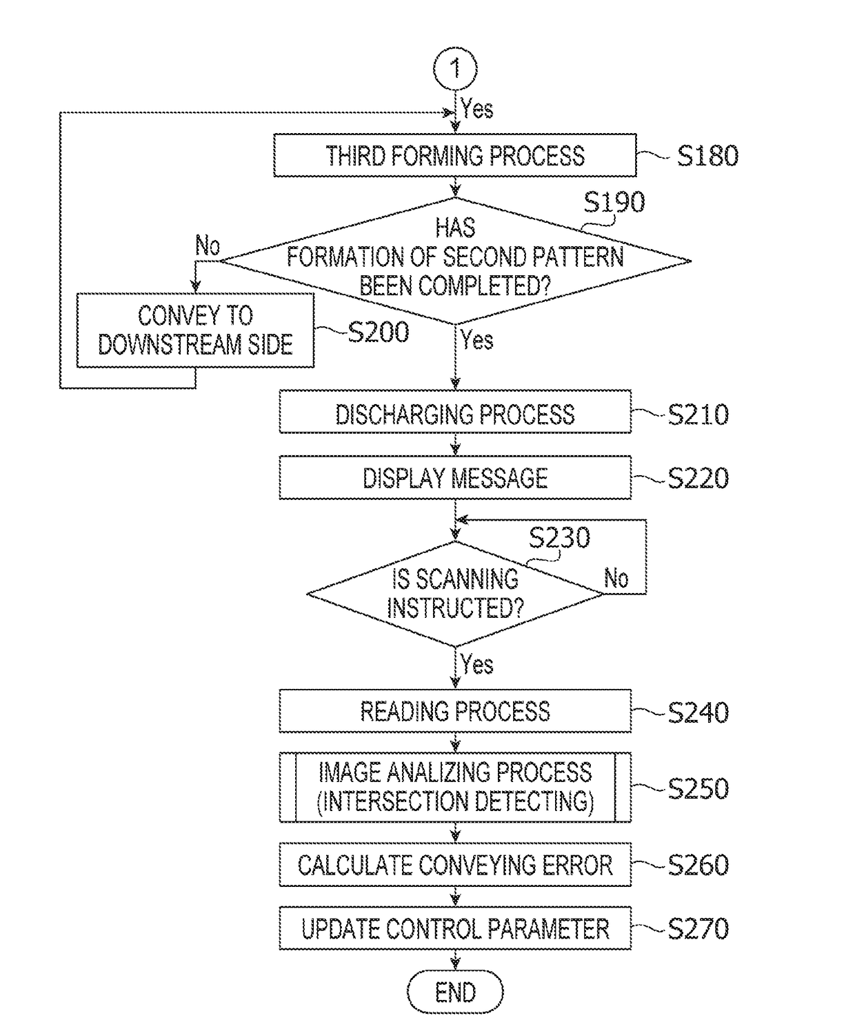
An electronic device is configured to acquire image data containing a test pattern including first and second patterns intersecting with each other. Pixels corresponding to the test pattern are determined by comparing brightness of each pixel with a threshold value, and widths of an overlapped image of the first and second patterns in an orthogonal direction at a plurality of different positions in the reference direction are calculated. Intersecting positions of the first pattern and the second pattern in the test pattern is detected based on a distribution of widths at the plurality of different positions. The test pattern has a model pattern having a set width in the orthogonal direction separate from the first and second patterns. The pixels corresponding to the test pattern are determined based on a threshold value, and widths at the plurality of positions of the overlapped image in the reference direction are calculated.

Description

CROSS-REFERENCE TO RELATED APPLICATIONS[0001]This application claims priority under 35 U.S.C. § 119 from Japanese Patent Application No. 2017-008915 filed on Jan. 20, 2017. The entire subject matter of the application is incorporated herein by reference.BACKGROUNDTechnical Field[0002]The present disclosures relate to an electronic device using a test pattern, a method of analyzing the test pattern, and a non-transitory recording medium storing computer-readable instructions to analyze the test pattern employed in the electronic device.Related Art[0003]There has been known an image forming system configured to form a test pattern on a sheet. The test pattern is formed in order to suppress a control error when an image is formed on a sheet, for example, an error in conveying the sheet. By suppressing the conveying error of the sheet, quality of an image formed on the sheet is improved. As the image forming system employing such a test pattern, there has been known serial printers such...

Claims


Application Information

Patent Timeline
IPC IPC(8): B41J29/393B41J11/00B41J2/04H04N1/00
CPCB41J29/393B41J11/008B41J2/04H04N1/00045H04N1/00588H04N1/00408H04N2201/0094B41J29/38B41J2/2135B41J13/0027B41J11/46
Inventor ARAI, YUSUKEHORADE, KENTAITO, TSUYOSHITERADA, KOHEISASO, TETSUYA
Owner BROTHER KOGYO KK
Learn More