Wideband antenna radiating element and method for producing wideband antenna radiating element
- Summary
- Abstract
- Description
- Claims
- Application Information
AI Technical Summary
Benefits of technology
Problems solved by technology
Method used
Image
Examples
first embodiment
[0110]Hereinafter, several types of wideband antenna radiating elements disposed in multilayer substrates according to the present invention will be described in details with reference to attached drawings. But, it would be well understood that this description should not be viewed as narrowing the appended claims.
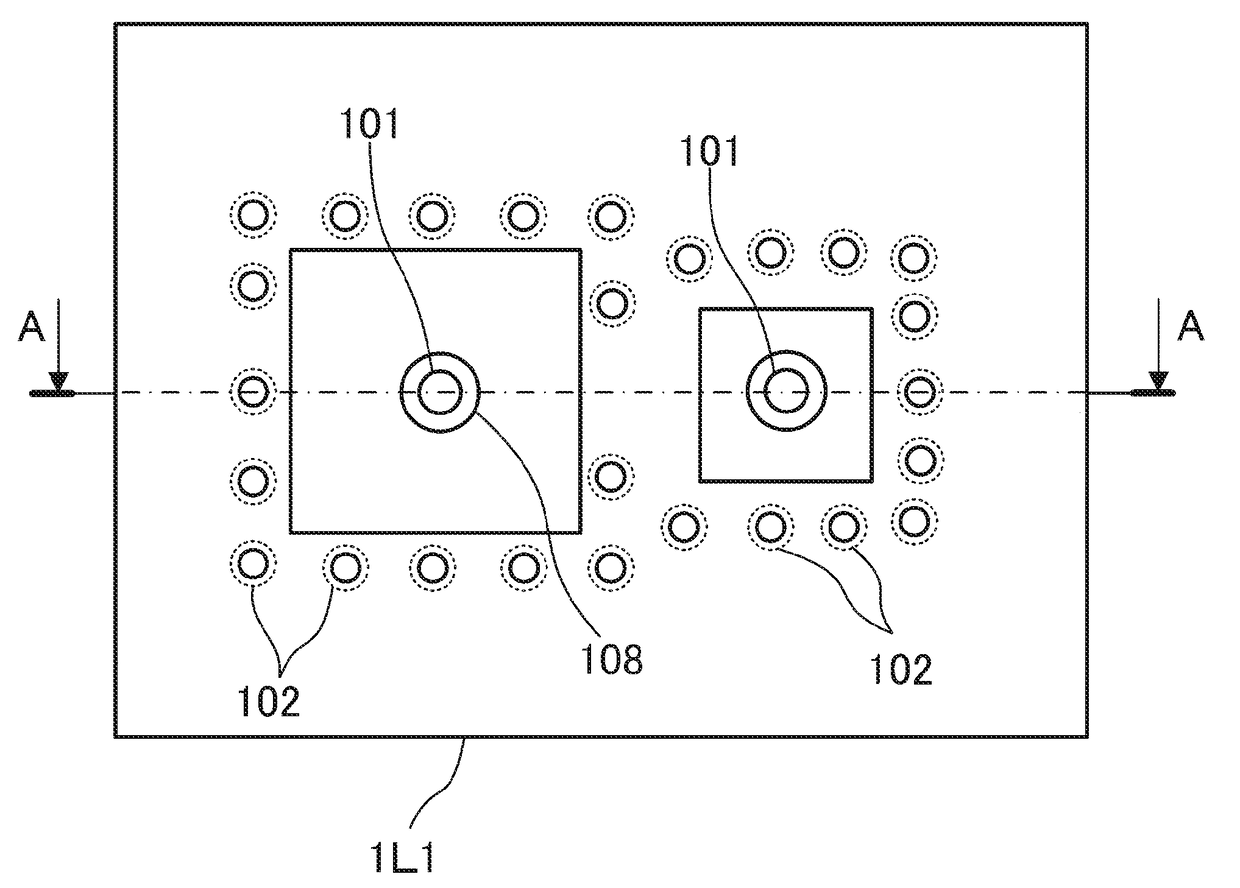
[0111]In FIGS. 1A to 1G, an exemplary embodiment of wideband antenna radiating element 110 disposed in a multilayer substrate is shown. This multilayer substrate is provided with a number of conductor layers 1L1 to 1L8. Eight conductor layers 1L1 to 1L8 are isolated by dielectric material 103.
[0112]Note this eight conductor layer substrate is only an example of multilayer substrates and a number of conductor layers, filling material and other substrate parameters can be different that depends on an application.
[0113]In the present embodiment, wideband antenna radiating element 110 is formed by two parts coupled with each other by coupling area 111. Each of said two parts c...
second embodiment
[0118]In FIGS. 2A to 2G, another exemplary embodiment of wideband antenna radiating element 210 disposed in a multilayer substrate is shown. This multilayer substrate is provided with a number of conductor layers 2L1 to 2L8. Eight conductor layers 2L1 to 2L8 are isolated by dielectric material 203.
[0119]In the present embodiment, wideband antenna radiating element 210 is formed by two parts coupled with each other by coupling area 211. In coupling area 211, an addition link between the two parts is carried out by slits 212 disposed in 2L2, 2L3, 2L4, 2L5, 2L6 and 2L7 conductor layers. Each of the two parts comprises signal via 201 and ground vias 202 surrounding signal via 201 and connected to ground conductor plates 209. Wideband antenna radiating element 210 has compact dimensions due to a high effective relative permittivity of an artificial medium which is formed between signal via 201 and ground vias 202 in each the part of wideband antenna radiating element 210. This artificial...
third embodiment
[0120]In FIGS. 3A to 3G, another exemplary embodiment of wideband antenna radiating element 310 disposed in a multilayer substrate is shown. This multilayer substrate is provided with a number of conductor layers 3L1 to 3L8. Eight conductor layers 3L1 to 3L8 are isolated by dielectric material 303.
[0121]In the present embodiment, wideband antenna radiating element 310 is formed by two parts coupled with each other by coupling area 311. In coupling area 311, an addition connection between the two parts is carried out by coupled strips 313 disposed in 3L3, 3L5, and 3L7 conductor layers. Each of the two parts comprises signal via 301 and ground vias 302 surrounding signal via 301 and connected to ground conductor plates 309. Wideband antenna radiating element 310 has compact dimensions due to a high effective relative permittivity of an artificial medium which is formed between signal via 301 and ground vias 302 in each the part of wideband antenna radiating element 310. This artificia...
PUM
 Abstract
Description
Claims
Application Information
 - R&D
- Intellectual Property
- Life Sciences
- Materials
- Tech Scout
- Unparalleled Data Quality
- Higher Quality Content
- 60% Fewer Hallucinations
Browse by: Latest US Patents, China's latest patents, Technical Efficacy Thesaurus, Application Domain, Technology Topic, Popular Technical Reports.
© 2025 PatSnap. All rights reserved.Legal|Privacy policy|Modern Slavery Act Transparency Statement|Sitemap|About US| Contact US: help@patsnap.com


