
Display device

a display device and display technology, applied in the direction of static indicating devices, instruments, etc., can solve the problems of difficult to compensate for variations, complex configuration of pixel circuits, and inconvenient operation of pixel circuits, so as to achieve uniform luminance to the entire screen

Active Publication Date: 2018-02-22
LG DISPLAY CO LTD
View PDF5 Cites 44 Cited by
  • Summary
  • Abstract
  • Description
  • Claims
  • Application Information

AI Technical Summary

Benefits of technology

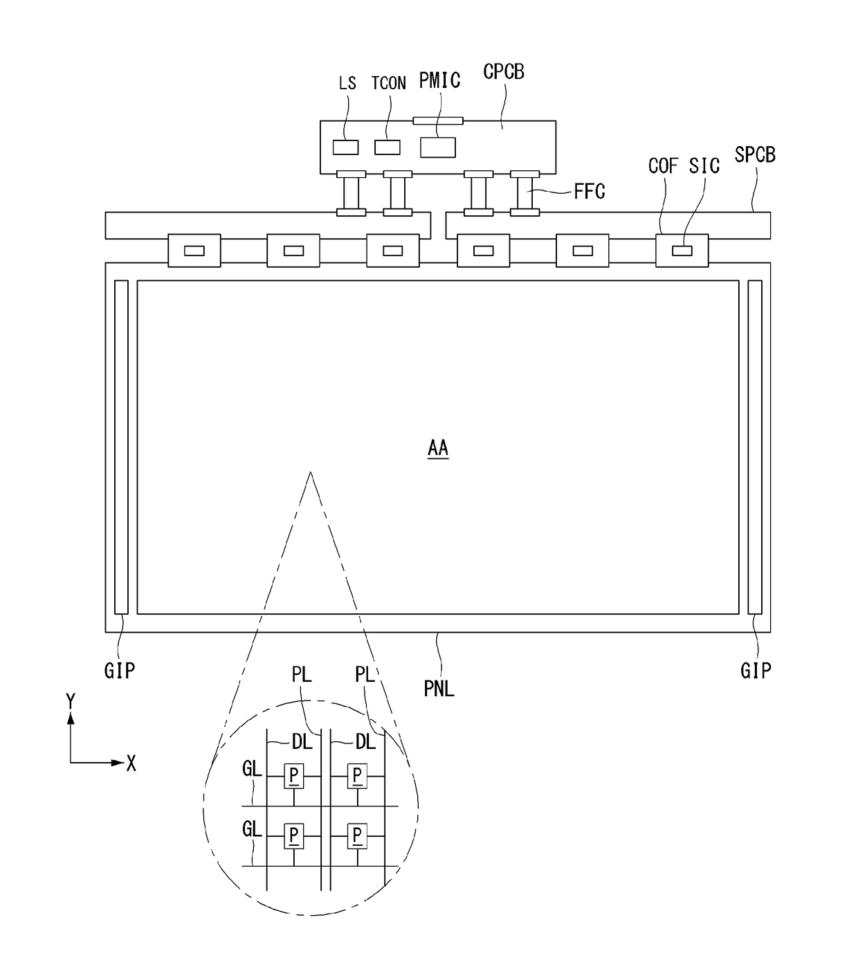
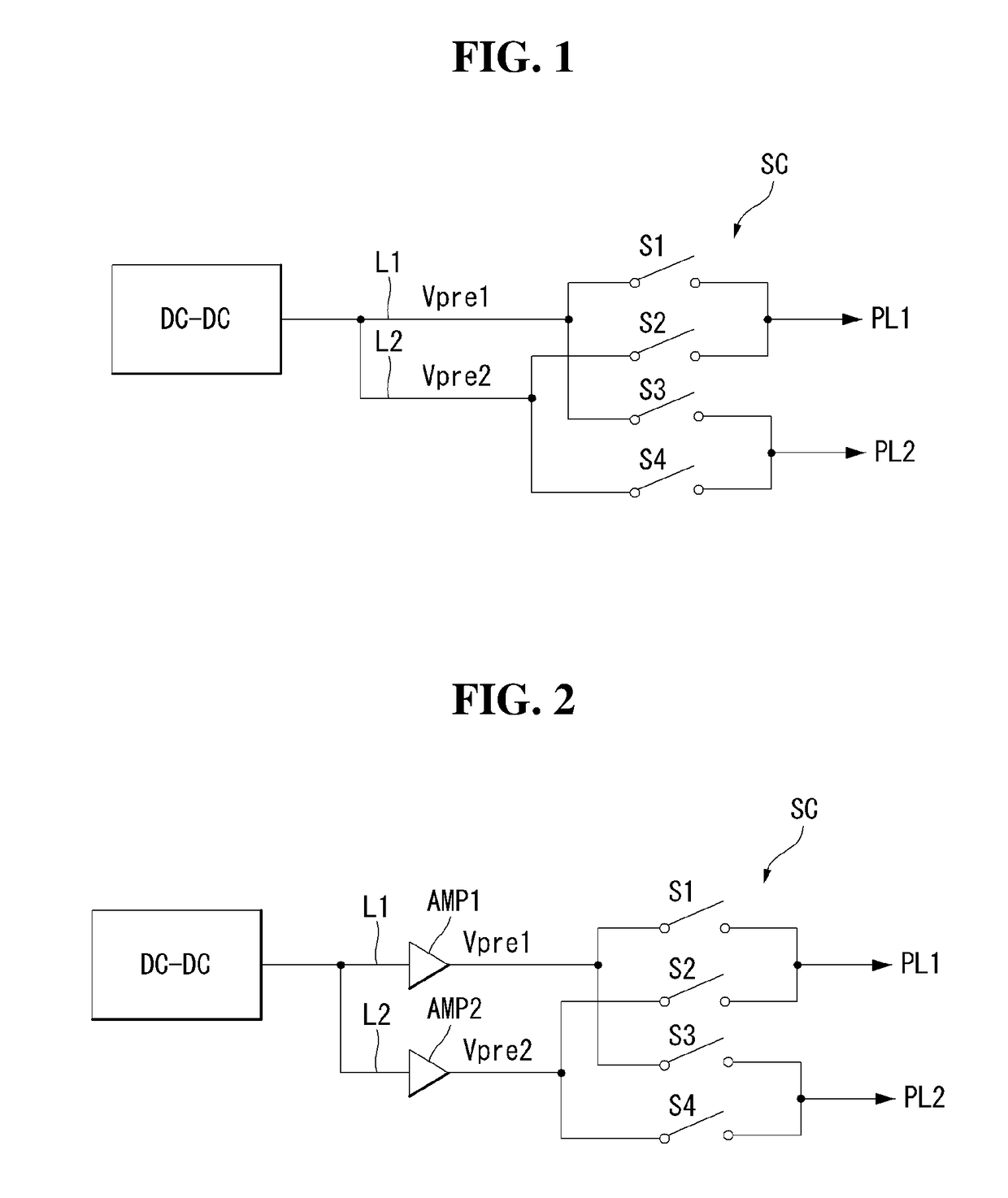
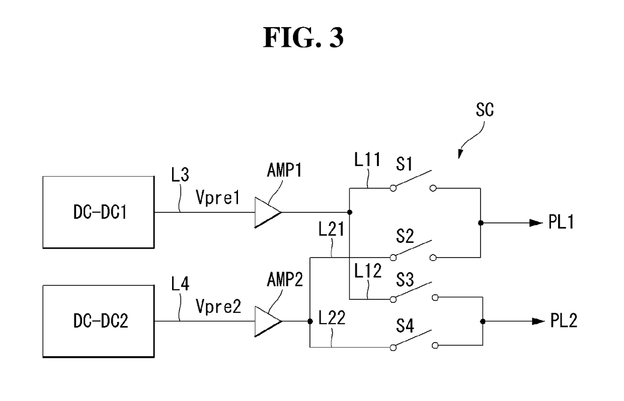
The patent text describes a display device and a method of driving it that can provide evenly distributed brightness across the entire screen, even if the reference voltage applied to the pixels is uneven. This is achieved by using a power circuit and a plurality of branch lines to divide the path of the reference voltage into multiple paths, which can be switched periodically to change the path between the branch lines and the panel lines. The technical effect of this invention is to improve the consistency and quality of display brightness across the entire screen.

Problems solved by technology

However, the electrical characteristics of the driving elements are not uniform due to process conditions, a driving environment, and the like.
Because the internal compensation method has to determine the current flowing in the OLED regardless of the threshold voltage of the driving element, configuration of the pixel circuit can be complicated.
Moreover, the internal compensation method is difficult to compensate for a variation in mobility between the driving elements.
When the level of the reference voltage varies as described above, the initialization of the pixels can be non-uniform.

Method used


Image

  • Display device
  • Display device
  • Display device

Examples


Embodiment Construction

[0048]Reference will now be made in detail to aspects of the present disclosure, examples of which are illustrated in the accompanying drawings. However, the present disclosure is not limited to aspects disclosed below, and may be implemented in various forms. These aspects are provided so that the present disclosure will be described more completely, and will fully convey the scope of the present disclosure to those skilled in the art to which the present disclosure pertains. Particular features of the present disclosure can be defined by the scope of the claims.

[0049]Shapes, sizes, ratios, angles, number, and the like illustrated in the drawings for describing aspects of the present disclosure are merely exemplary, and the present disclosure is not limited thereto unless specified as such. Like reference numerals designate like elements throughout. In the following description, when a detailed description of certain functions or configurations related to this document that may unn...


PUM


Abstract

A display device is disclosed. The display device includes a display panel including data lines, panel lines, scan lines, and pixels, a power circuit configured to output a reference voltage for initializing subpixels of the pixels, a plurality of branch lines configured to divide a path of the reference voltage into a plurality of paths, and a switch circuit configured to switch a path between the branch lines and the panel lines in response to a switch control signal. The switch circuit changes the path between the branch lines and the panel lines at intervals of predetermined time.

Description

CROSS-REFERENCE TO RELATED APPLICATION[0001]This application claims the benefit of Korean Patent Application No. 10-2016-0104456 filed on Aug. 17, 2016, the entire contents of which is incorporated herein by reference in its entirety for all purposes as if fully set forth herein.BACKGROUNDField of the Disclosure[0002]The present disclosure relates to a display device and more particularly, to a display device capable of providing uniform luminance to the entire screen even if a level of a reference voltage applied to pixels is non-uniform.Description of the Background[0003]An active matrix organic light emitting diode (OLED) display includes a plurality of OLEDs capable of emitting light by themselves and has many advantages, such as fast response time, high emission efficiency, high luminance, wide viewing angle, and the like. The OLED includes an anode, a cathode, and an organic compound layer between the anode and the cathode. The organic compound layer includes a hole injection ...

Claims


Application Information

Patent Timeline
Patent Type & Authority Applications(United States)
IPC IPC(8): G09G3/20G09G3/3233
CPCG09G3/2074G09G3/3233G09G2310/08G09G2320/045G09G2300/0819G09G2300/043G09G2320/0233G09G2300/0426G09G2310/0251G09G2320/0223G09G2320/0295G09G2300/0828G09G2310/061G09G2230/00G09G2330/028
Inventor BAE, HANJINYU, SANGHO
Owner LG DISPLAY CO LTD
Learn More