
Display panel, display device, and method for manufacturing display panel

a display panel and display device technology, applied in non-linear optics, instruments, optics, etc., can solve the problems of data line short circuit, etc., and achieve the effect of easy short circuit and high ng rate of produ

Active Publication Date: 2018-02-15
BOE TECH GRP CO LTD +1
View PDF3 Cites 0 Cited by
  • Summary
  • Abstract
  • Description
  • Claims
  • Application Information

AI Technical Summary

Benefits of technology

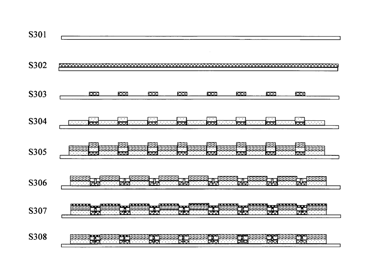
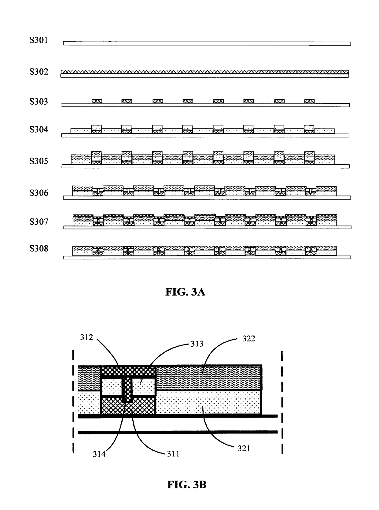
The present invention provides a display panel, display device, and method for manufacturing a display panel that can prevent data lines from short-circucling and reduce the NG rate of the product. This is achieved by providing a substrate in the electrode region of the display panel and a data line layer and isolation layer that are alternated with each other in a direction parallel to the upper surface of the substrate so that the height of the data line layer is equal to the height of the isolation layer. This reduces short-circuiting caused by tilting of data lines and improves product yield per product.

Problems solved by technology

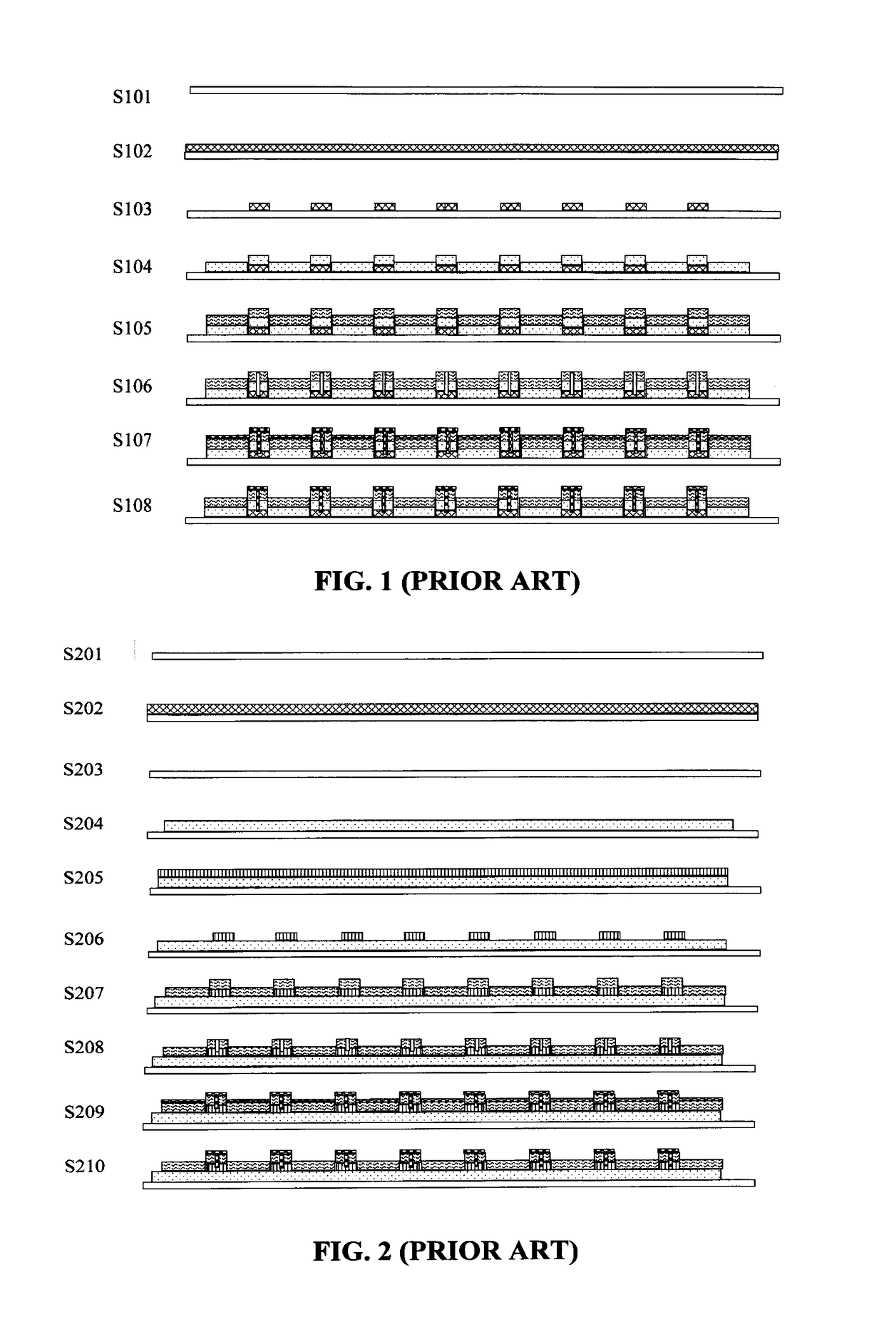
First, since a data line layer is higher than an adjacent insulating layer, foreign objects are accumulated in the insulating layer when the electrode region is cleaned, and when foreign objects too many are accumulated, a short circuit is caused among the data lines.
Second, since the data line layer is higher than the adjacent insulating layer, the data lines might be caused to tilt toward the insulating layer due to pressure reason or loose array coating during the cleaning of the electrode region, and when too many foreign objects are accumulated, a short circuit is caused between the data lines.

Method used


Image

  • Display panel, display device, and method for manufacturing display panel
  • Display panel, display device, and method for manufacturing display panel
  • Display panel, display device, and method for manufacturing display panel

Examples


Embodiment Construction

[0048]To make the technical solutions and advantages of the present disclosure clearer, the technical solutions of the embodiments of the present disclosure will be clearly and completely described below in conjunction with the drawings. Obviously, the embodiments described are part of embodiments of the present disclosure, instead of all the embodiments. Based on the described embodiments of the present disclosure, all other embodiments obtained by those skilled in the art without creative work also fall within the scope of protection sought for by the present disclosure.

[0049]When describing elements of the present disclosure and embodiments thereof, the articles “a”, “an”, “the” and “said” are intended to mean the presence of one or more elements. The terms “including”, “comprising”, “containing” and “having” are intended to be inclusive and to indicate that there may be additional elements other than the listed elements.

[0050]For the purpose of the literal description below, the...


PUM

PropertyMeasurementUnit
heightaaaaaaaaaa
conductiveaaaaaaaaaa
insulatingaaaaaaaaaa

Abstract

The present disclosure relates to a display panel, a display device, and a method for manufacturing a display panel. The display panel has an electrode region, the electrode region including a substrate, a data line layer, and an isolation layer which are provided on the substrate and alternated in a direction parallel to an upper surface of the substrate, wherein the height of the data line layer is equal to the height of the isolation layer. Since there is no height difference between the data line layer and the spacer layer and there is no groove, the possibility that conductive foreign objects are accumulated at the isolation layer at this time is greatly reduced, the smooth surface is more conducive to the movement of foreign objects, and a cleaning tape can remove the foreign objects.

Description

CROSS REFERENCE TO RELATED APPLICATIONS[0001]This patent application is a National Stage Entry of PCT / CN2016 / 084243 filed on Jun. 1, 2016, which claims the benefit and priority of Chinese Patent Application No. 201610117900.3 filed on Mar. 2, 2016, the disclosures of which are incorporated herein in their entirety as a part of the present application.BACKGROUND[0002]The present disclosure relates to the technical field of display, and in particular, to a display panel, a display device, and a method for manufacturing a display panel.[0003]There are generally four processes to produce a liquid crystal panel: array process, color filter (CF) process, cell process, and module process. The coating of electrode region (Pad) is completed in the array process, and the attaching of COF and PCB is completed in the module process. Before the attaching process in the module process is performed, the electrode region is pressure-cleaned using a cleaning tape.[0004]Under existing technical condi...

Claims


Application Information

Patent Timeline
Patent Type & Authority Applications(United States)
IPC IPC(8): G02F1/1343G02F1/1333G02F1/1339
CPCG02F1/1343G02F1/1339G02F1/133345G02F1/1333G02F1/136286G02F1/13629G02F1/136204G02F1/136295
Inventor WANG, HEWEIHAN, LEIJIANG, PENGGUO, DONGZHANG, NANHONG
Owner BOE TECH GRP CO LTD
Learn More