Configurable Gate Array Based on Three-Dimensional Writable Memory

a three-dimensional writable memory and configurable technology, applied in the field of integrated circuits, can solve the problems of limiting further applications of configurable gate arrays, and achieve the effects of reducing die cost, reducing processing power, and reducing the size of dies

Inactive Publication Date: 2018-02-08
HANGZHOU HAICUN INFORMATION TECH +1
View PDF1 Cites 1 Cited by
  • Summary
  • Abstract
  • Description
  • Claims
  • Application Information

AI Technical Summary

Benefits of technology

[0006]It is a principle object of the present invention to extend the applications of a configurable gate array to the field of complex math computation.
[0007]It is a further object of the present invention to provide a configurable gate array where not only logic functions can be customized, but also math functions.
[0008]It is a further object of the present invention to provide a configurable gate array with more computing power.
[0009]It is a further object of the present invention to provide a configurable gate array with smaller die size and lower die cost.
[0010]In accordance with these and other objects of the present invention, the present invention discloses a configurable gate array based on three-dimensional writable memory (3D-W).
[0011]The present invention discloses a configurable gate array based on three-dimensional writable memory (3D-W). It comprises an array of configurable computing elements, an array of configurable logic elements and an array of configurable interconnects. Each configurable computing element comprises at least a 3D-W array, which is electrically programmable and can be loaded with a look-up table (LUT) for a math function. The usage cycle of the configurable computing element comprises two stages: a configuration stage and a computation stage. In the configuration stage, the LUT for a desired math function is loaded into the 3D-W array. In the computation stage, the functional value of the desired math function is read out from the LUT. For an electrically re-programmable 3D-W, a configurable computing element can be re-configured to realize different math functions.

Problems solved by technology

Apparently, fixed computing elements would limit further applications of the configurable gate array.

Method used


Image

  • Configurable Gate Array Based on Three-Dimensional Writable Memory
  • Configurable Gate Array Based on Three-Dimensional Writable Memory
  • Configurable Gate Array Based on Three-Dimensional Writable Memory

Examples


Embodiment Construction

[0029]Those of ordinary skills in the art will realize that the following description of the present invention is illustrative only and is not intended to be in any way limiting. Other embodiments of the invention will readily suggest themselves to such skilled persons from an examination of the within disclosure.

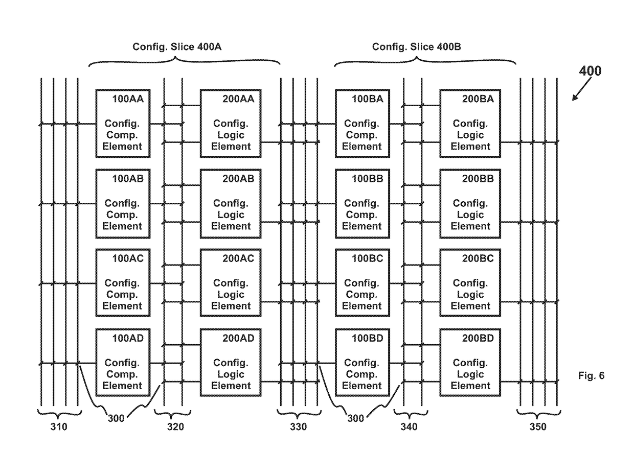
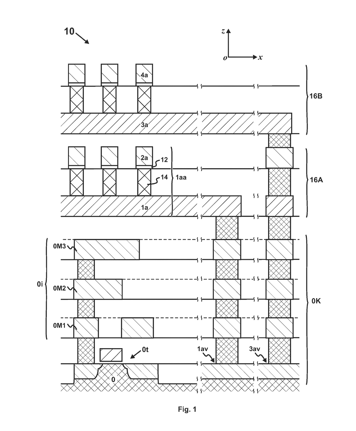
[0030]Referring now to FIG. 1, a preferred three-dimensional writable memory (3D-W) 10 is shown. 3D-W is a type of three-dimensional memory (3D-M) whose memory cells are electrically programmable. Based on the number of programming allowed, a 3D-W can be categorized into three-dimensional one-time-programmable memory (3D-OTP) and three-dimensional multiple-time-programmable memory (3D-MTP). Types of the 3D-MTP cell include flash-memory cell, memristor, resistive random-access memory (RRAM or ReRAM) cell, phase-change memory (PCM) cell, programmable metallization cell (PMC), conductive-bridging random-access memory (CBRAM) cell, and the like.

[0031]Based on the orientation of...


PUM


Abstract

The present invention discloses a configurable gate array based on three-dimensional writable memory (3D-W). It comprises an array of configurable computing elements, an array of configurable logic elements and an array of configurable interconnects. Each configurable computing element comprises at least a 3D-W array, which is electrically programmable and can be loaded with a look-up table (LUT) for a math function.

Description

CROSS-REFERENCE TO RELATED APPLICATIONS[0001]This application is a continuation-in-part of U.S. patent application Ser. No. 15 / 450,049, filed Mar. 6, 2017, which is a continuation-in-part of U.S. patent application Ser. No. 15 / 450,017, filed Mar. 5, 2017. These patent applications claim priorities from Chinese Patent Application No. 201610125227.8, filed Mar. 5, 2016; Chinese Patent Application No. 201610307102.7, filed May 10, 2016, in the State Intellectual Property Office of the People's Republic of China (CN).[0002]This application also claims priorities from Chinese Patent Application No. 201710122749.7, filed Mar. 3, 2017; Chinese Patent Application No. 201710942493.4, filed Oct. 11, 2017, in the State Intellectual Property Office of the People's Republic of China (CN), the disclosure of which are incorporated herein by reference in their entireties.BACKGROUND1. Technical Field of the Invention[0003]The present invention relates to the field of integrated circuit, and more par...

Claims


Application Information

Patent Timeline
Patent Type & Authority Applications(United States)
IPC IPC(8): H03K19/177G11C5/02
CPCH03K19/1776H03K19/17728H03K19/17744G11C5/02G11C5/025H03K19/1737
Inventor ZHANG, GUOBIAO
Owner HANGZHOU HAICUN INFORMATION TECH
Why Eureka
Try Eureka