Array substrate and fabrication method, display panel, and display device

a technology of array substrate and substrate, applied in the field of touch control technologies, can solve the problems of complex pixel circuit, high ppi display structure wiring layout, and increasing complexity of pixel circui

Active Publication Date: 2017-10-05
WUHAN TIANMA MICRO ELECTRONICS CO LTD +1
View PDF7 Cites 3 Cited by
  • Summary
  • Abstract
  • Description
  • Claims
  • Application Information

AI Technical Summary

Benefits of technology

This patent is about improving the design of array substrates for display panels. The technical effects of the patent include avoiding problems caused by variations in through-hole depth and making the layout process easier for high-pixel display substrates. The patent also addresses the issue of wider diameter through-holes requiring wider metal layers to properly connect, which can interfere with wiring layouts. Overall, the patent provides a solution to improve the quality and efficiency of array substrates for display panels.

Problems solved by technology

However, at the same time, the pixel circuits are getting more and more complicated.
The complicated pixel circuits and the wiring layout of high PPI display structures become a great challenge to the fabrication process and equipment.

Method used


Image

  • Array substrate and fabrication method, display panel, and display device
  • Array substrate and fabrication method, display panel, and display device
  • Array substrate and fabrication method, display panel, and display device

Examples


Embodiment Construction

[0030]Reference will now be made in detail to exemplary embodiments of the disclosure, which are illustrated in the accompanying drawings. Wherever possible, the same reference numbers will be used throughout the drawings to refer to the same or like parts. It should be understood that the exemplary embodiments described herein are only intended to illustrate and explain the present invention and not to limit the present invention.

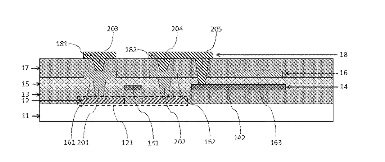
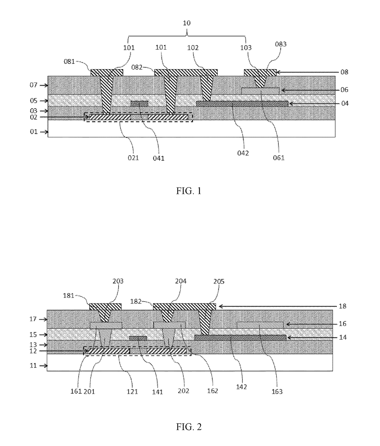
[0031]In a display pane, pixel driving circuits may include a plurality of thin film transistors (TFT) arranged in an array and a plurality of signal lines that are located between the TFTs and carry the control signals to control individual TFT. The TFTs may be multi-layer structures including a plurality of active layer, gate electrode layer, source and drain electrode layer. The signal lines may often be disposed on the top layer of the TFT array substrate, and may be coplanar with the source and drain electrodes of the TFTs. As the PPI increases and th...


PUM

PropertyMeasurementUnit
thicknessaaaaaaaaaa
thicknessaaaaaaaaaa
thicknessaaaaaaaaaa

Abstract

The present disclosure provides an array substrate, including a substrate, a first functional layer configured on one side of the substrate, a first insulating layer configured on the first functional layer facing away from the substrate, a second functional layer configured on the first insulating layer facing away from the substrate, a second insulating layer configured on the second functional layer facing away from the substrate, a third functional layer configured on the second insulating layer facing away from the substrate, a third insulating layer configured on the third functional layer facing away from the substrate, a fourth functional layer configured on the third insulating layer facing away from the substrate, and a plurality of through-holes configured to electrically connect different functional layers, wherein the depth of any through-holes does not exceed the thickness of two adjacent insulating layers.

Description

CROSS-REFERENCES TO RELATED APPLICATIONS[0001]This application claims the priority of Chinese Patent Application No. CN201610200728.8, filed on Mar. 31, 2016, the entire contents of which are incorporated herein by reference.FIELD OF THE DISCLOSURE[0002]The present disclosure generally relates to the touch control technologies and, more particularly, relates to an array substrate, a fabrication method thereof, a display panel incorporating the array substrate, and a display device incorporating the display panel.BACKGROUND[0003]Today, with advances in technologies, people are demanding more from the display technology. The display resolutions have been increasing gradually. High definition, ultra high definition, full high definition, retina technology, 2K, 4K, 8K, 10K, and other display technology terms are getting into people's daily life.[0004]PPI (pixels per inch), a measurement of pixel density or resolution, represents the number of pixels per inch. The higher the PPI value, t...

Claims


Application Information

Patent Timeline
Patent Type & Authority Applications(United States)
IPC IPC(8): H01L27/12G02F1/1362G02F1/1335H01L29/786H01L21/77
CPCH01L27/1244H01L27/1222H01L27/1255H01L27/127H01L27/3262H01L29/78675G02F1/136227G02F1/133514H01L27/1288H01L21/77H01L27/124H01L27/1259H01L2021/775G02F1/13685H10K59/1213
Inventor LI, QIQIAN, DONGPENG, DUZEN
Owner WUHAN TIANMA MICRO ELECTRONICS CO LTD
Why Eureka
Try Eureka