Method of Carrier Profiling Utilizing Dielectric Relaxation

Active Publication Date: 2017-07-13
HAGMANN MARK J
View PDF3 Cites 3 Cited by
  • Summary
  • Abstract
  • Description
  • Claims
  • Application Information

AI Technical Summary

Benefits of technology

The invention provides a new way to measure the electrical properties of carriers in a material using a method called dielectric relaxation. This method is easier to do, uses existing equipment, and can provide quantitative results with minimal calibration. It is also non-destructive and can be repeated using the same samples. This new method can help to improve the quality and accuracy of carrier profiling in various fields such as electronics and biotechnology.

Problems solved by technology

However, in laser-assisted scanning tunneling microscopy there is also an inelastic contribution to the tunneling current [N. M. Miskovsky, S.-H.
Furthermore, a reverse-biased tunneling junction would cause a depletion region that would interfere with the transport within the semiconductor.

Method used


Image

  • Method of Carrier Profiling Utilizing Dielectric Relaxation
  • Method of Carrier Profiling Utilizing Dielectric Relaxation
  • Method of Carrier Profiling Utilizing Dielectric Relaxation

Examples


Embodiment Construction

[0028]With reference now to the drawings, the preferred embodiment of the method is herein described. It should be noted that the articles “a,”“an,” and “the” as used in this specification, include plural referents unless the content clearly dictates otherwise.

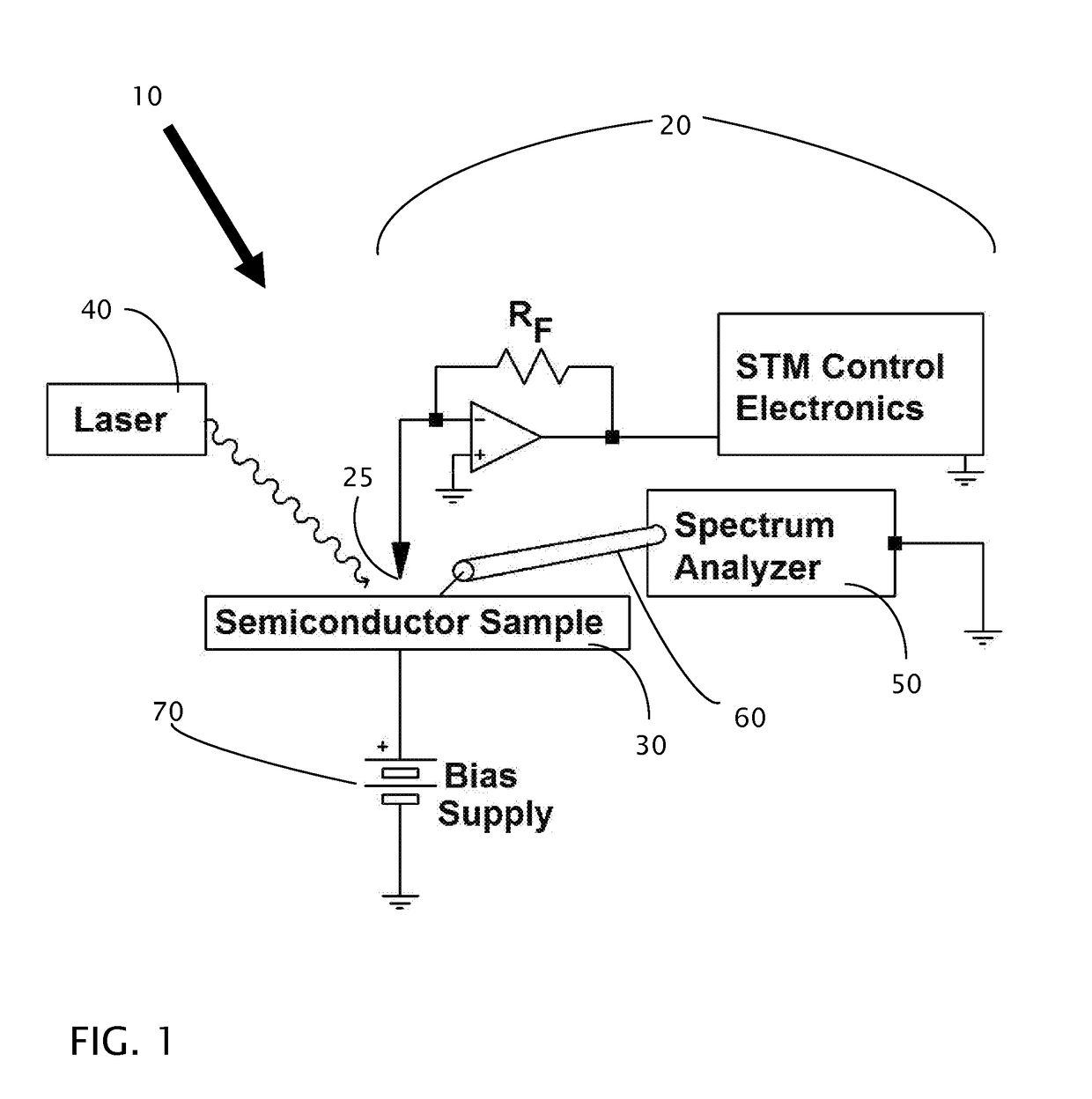
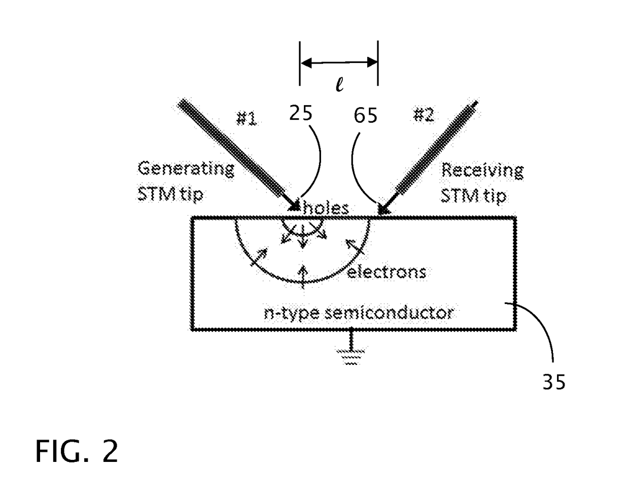
[0029]With reference to FIG. 1, a scanning tunneling microscope is set up similarly to what is described in U.S. Pat. No. 9,442,078 (2016), also by this Inventor. This Patent is incorporated by reference in its entirety herein. In one embodiment, an apparatus set-up 10 is a scanning tunneling microscope 20 positioned over a sample 30 onto which a mode-locked laser 40 is focused so that the laser emits a beam onto the tunneling junction between the STM 20 and the sample 30. The semiconductor sample 30 is forward biased 70, as is shown in FIG. 1 where a p-type semiconductor 30 is used and the voltage on the STM tip 25 is set to make the tip negative, thus allowing the carriers in the semiconductor sample to remain in the region ...


PUM


Abstract

A mode-locked laser injects pulses of minority carriers into a semiconductor sample. A microwave frequency comb is then generated by the currents formed in the movement of majority carriers native to the semiconductor and the injected minority carriers. These carriers move to cause dielectric relaxation in the sample, which can be used to determine carrier density within the sample. Measurements require close proximity of transmitter and receiver contacts with the sample and may profile a semi-conductor with a resolution of approximately 0.2 nm.

Description

CROSS-REFERENCES TO RELATED APPLICATIONS[0001]This Application claims priority as a non-provisional perfection of prior filed U.S. Application No. 62 / 276,678, filed Jan. 8, 2016, and incorporates the same by reference in its entirey.FIELD OF THE INVENTION[0002]The present invention relates to the field of carrier profiling in conductors and semiconductors and more particularly relates to a method by which a microwave frequency comb is used to measure dielectric relaxation in order to determine carrier density.BACKGROUND OF THE INVENTION[0003]Round-robin testing and status reviews have led the semiconductor industry to select scanning spreading resistance microscopy (SSRM) and scanning capacitance microscopy (SCM) as their primary methods for carrier profiling. SSRM is generally chosen below the 40 nm lithography node where finer resolution is required. The resolution for SSRM is thought to be as fine as 2.5 nm [K. Arstila, T. Hantschel, C. Demeulemeester, A. Moussa and W. Vandervors...

Claims


Application Information

Patent Timeline
IPC IPC(8): G01Q60/10
CPCG01Q60/10G01Q60/12
Inventor HAGMANN, MARK J.
Owner HAGMANN MARK J
Why Eureka
Try Eureka