Package structure for a high-frequency electronic component
- Summary
- Abstract
- Description
- Claims
- Application Information
AI Technical Summary
Benefits of technology
Problems solved by technology
Method used
Image
Examples
first embodiment
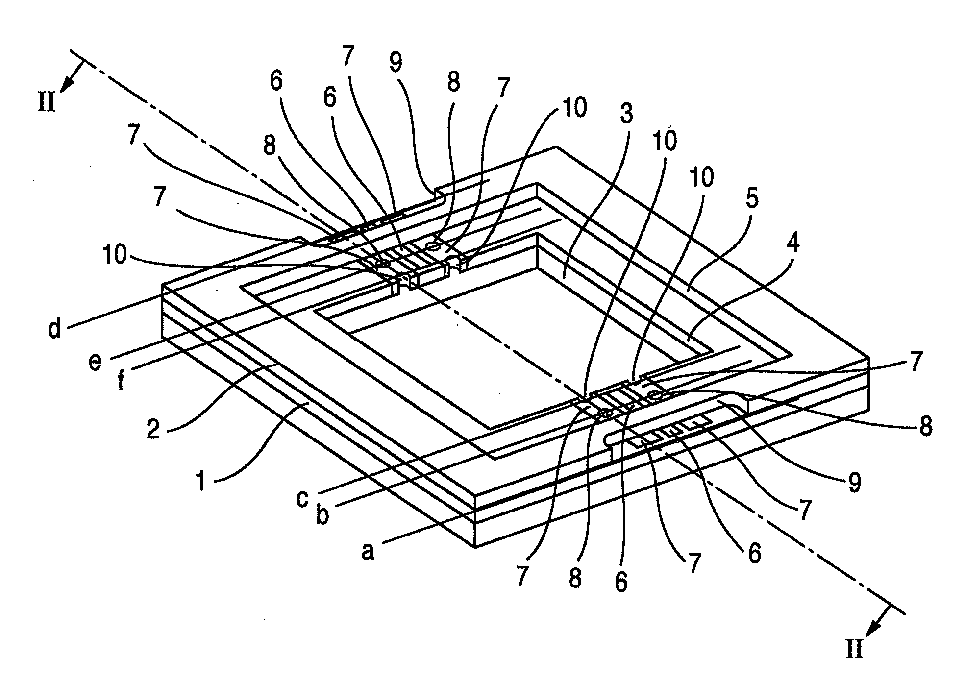
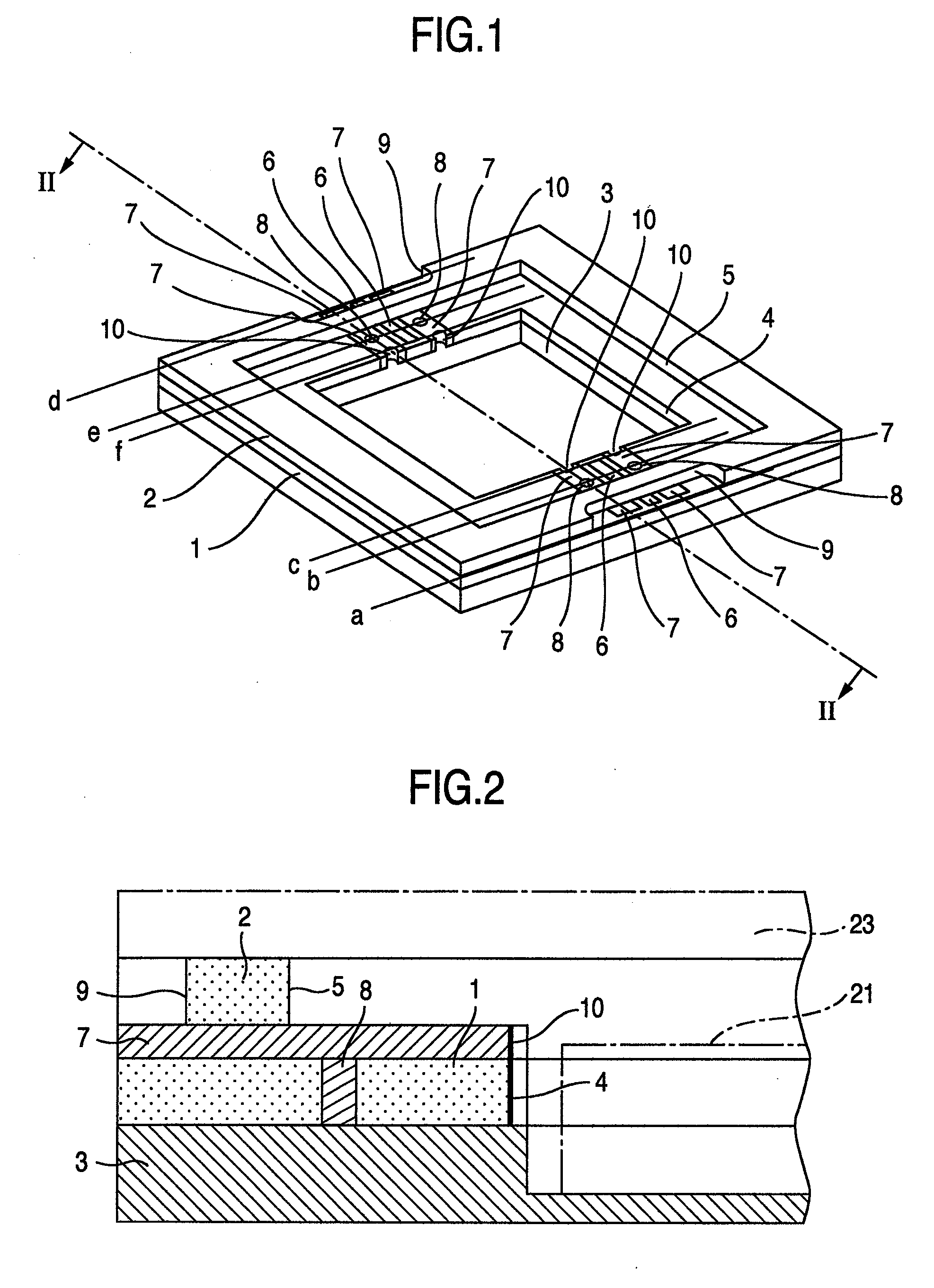
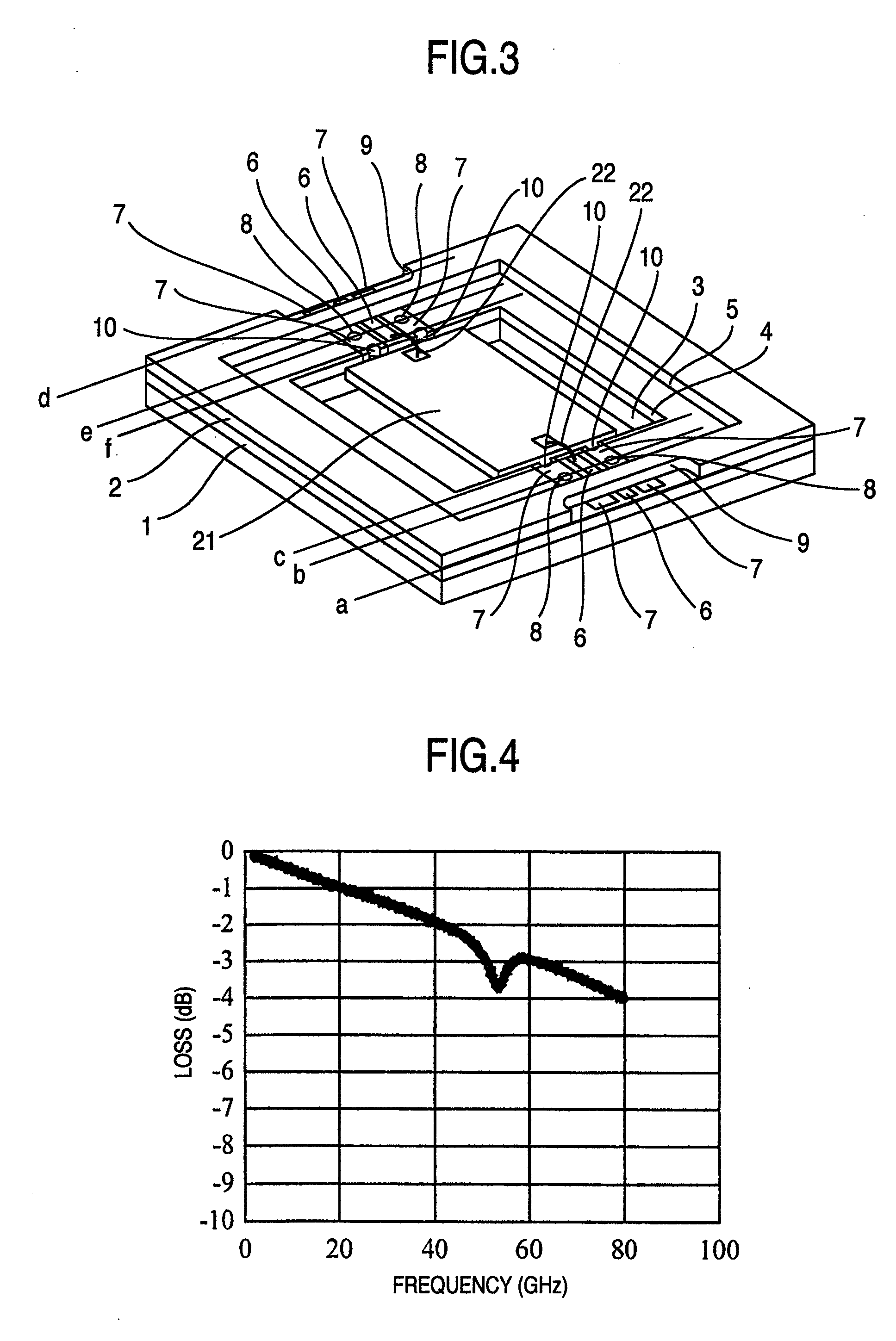
[0052]FIG. 1 shows a package structure for a high-frequency electronic component, the package structure being associated with the present invention. FIG. 2 shows a cross-sectional structure of one of electrode lines 7 for grounding.
[0053]In the embodiments described below, a dielectric substrate is used as a dielectric member. A metal enclosure for grounding or a dielectric substrate coated with a metal is used as an electric conductor for grounding.
[0054]In FIGS. 1 and 2, a first layer of dielectric substrate 1 is provided with a hole (hollow space or compartment) 4 of a cavity structure. The hole 4 accommodates an electronic component 21. Conductive transmission lines (traces) 6 and a pair of electrode lines (traces) 7 for grounding which together form a distributed constant element are formed on the top surface of the dielectric substrate 1. A metal enclosure 3 for grounding is formed on the bottom surface of the dielectric substrate 1, thus forming a bottom surface for the hole ...
second embodiment
[0070]Thus, in the second embodiment as well, the electrode lines 7 for grounding are connected at their intermediate portions with the metal enclosure 3 for grounding via the conductive through-holes 8, the intermediate portions extending from the base ends of the electrode lines 7 to the front ends and the electrode lines 7 are also connected at their front ends with the metal enclosure 3 for grounding by the metal conductors 11. Alternatively, it is also possible to connect the electrode lines 7 for grounding with the metal enclosure 3 for grounding by the metal conductors 11 without forming the conductive through-holes 8.
[0071]The transmission characteristics of the sections a-c and d-f (FIG. 6) of the package structure according to the second embodiment are similar to the transmission characteristics (FIG. 4) of the package structure according to the first embodiment. Similarly, the reflection characteristics of the sections a-c and d-f are similar to the reflection characteris...
third embodiment
[0075]In the package structure for use with a high-frequency electronic component and built the hole formed in the second layer of dielectric substrate 3b cooperates with the hole 4 formed in the third layer of dielectric substrate 1 to form a recessed portion of the cavity structure for accommodating the electronic component 21.
[0076]In the third embodiment, the front ends of the electrode lines 7 for grounding formed on the dielectric substrate 1 and facing the recessed portion are connected with the metal surface on the second layer of dielectric substrate 3b through the semicylindrical through-holes 10. Consequently, the front ends of the electrode lines 7 for grounding are connected with the grounding surface consisting of two layers of dielectric substrates 3a and 3b which are totally deposited with metal in their entirety.
[0077]Furthermore, in the third embodiment, to take out a high-frequency signal to the outside or accepting the signal, semicylindrical through-holes 13 an...
PUM
 Abstract
Description
Claims
Application Information
 - R&D
- Intellectual Property
- Life Sciences
- Materials
- Tech Scout
- Unparalleled Data Quality
- Higher Quality Content
- 60% Fewer Hallucinations
Browse by: Latest US Patents, China's latest patents, Technical Efficacy Thesaurus, Application Domain, Technology Topic, Popular Technical Reports.
© 2025 PatSnap. All rights reserved.Legal|Privacy policy|Modern Slavery Act Transparency Statement|Sitemap|About US| Contact US: help@patsnap.com


