
Wire grid polarizer and manufacturing method thereof, display panel and display device

a technology of wire grid polarizer and manufacturing method, which is applied in the field of display, can solve the problems of low light utilization of lcd and the development of display panels to improve light utilization, so as to avoid peripheral light leakage, reduce light absorption rate, and control more flexibly

Active Publication Date: 2016-12-08
BOE TECH GRP CO LTD
View PDF13 Cites 12 Cited by
  • Summary
  • Abstract
  • Description
  • Claims
  • Application Information

AI Technical Summary

Benefits of technology

The invention provides a wire grid polarizer and a manufacturing method, a display panel, and a display device. The wire grid polarizer has wire grid structures arranged at intervals in an array. The display panel can effectively lower the light absorption rate, prevent peripheral light leakage, and avoid pixels' light leakage. The wire grid polarizer allows for flexible control of light beam emergence, and the display panel and display device using it can improve light utilization rate and achieve a good display effect.

Problems solved by technology

In general, the lower polarizer can only allow penetration of light of no more than 50%, with the rest being absorbed, thus causing low light utilization of the LCD.
Therefore, designing a display panel to improve the light utilization has now become an urgent technical problem that need to be solved.

Method used


Image

  • Wire grid polarizer and manufacturing method thereof, display panel and display device
  • Wire grid polarizer and manufacturing method thereof, display panel and display device
  • Wire grid polarizer and manufacturing method thereof, display panel and display device

Examples


embodiment 1

[0043]The embodiment provides a wire grid polarizer, which has wire grid structures arranged at intervals, thus forming local light transmitting areas, so as to be able to control the emergence of light beams.

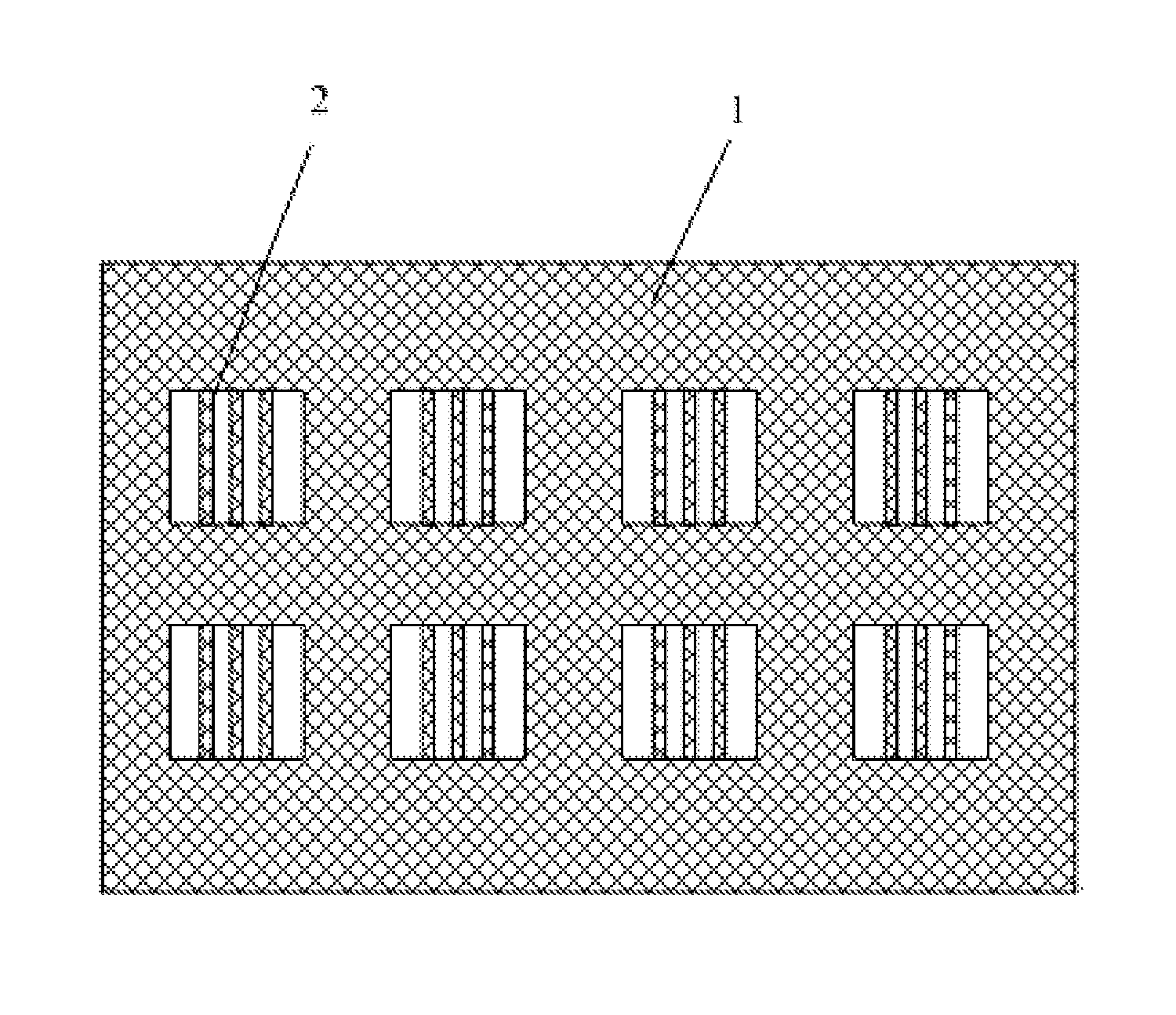
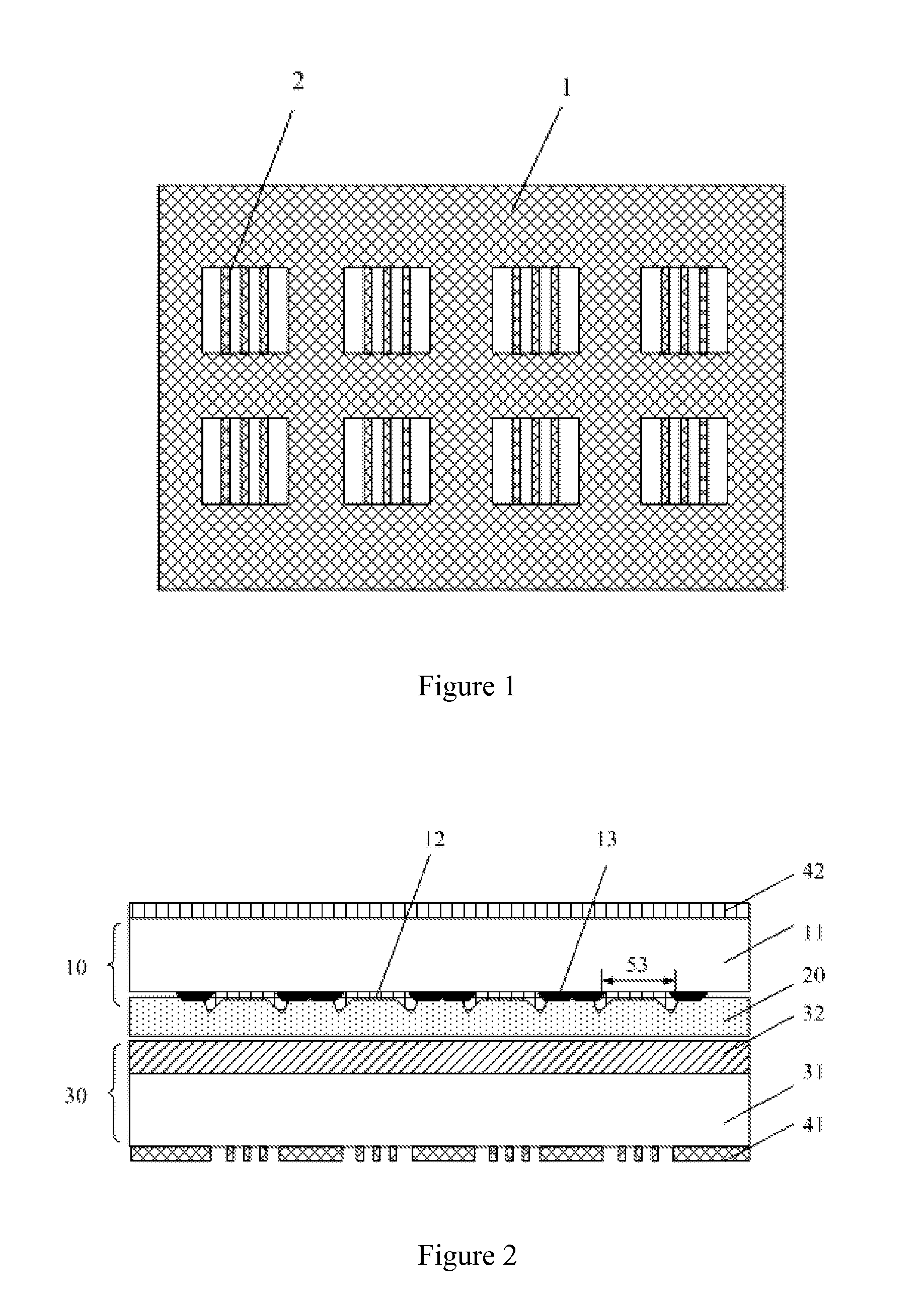
[0044]As shown in FIG. 1, the wire grid polarizer comprises a substrate 1, on which are formed multiple open areas arranged at intervals in an array. The wire grid polarizer also comprises multiple WG structures 2 disposed in the multiple open areas respectively, each of the WG structures 2 comprising multiple grid lines arranged at intervals, the intervals between two adjacent grid lines forming the grid pitches of the WG structures 2. Due to the WG structures 2, light can penetrate through the grid pitches of the WG structures 2. The area, except the open areas, of the substrate is a continuous opaque area.

[0045]The thickness of the substrate 1 ranges 20-250 nm Preferably, in the WG structures 2, the width of the grid lines ranges 25-250 nm, and the width of the grid pitches ...

embodiment 2

[0064]This embodiment provides a display panel comprising the wire grid polarizer of embodiment 1. The display panel can effectively reduce the light absorption rate, and can also avoid the peripheral light leakage in a non-subpixel area, thus having a better display effect.

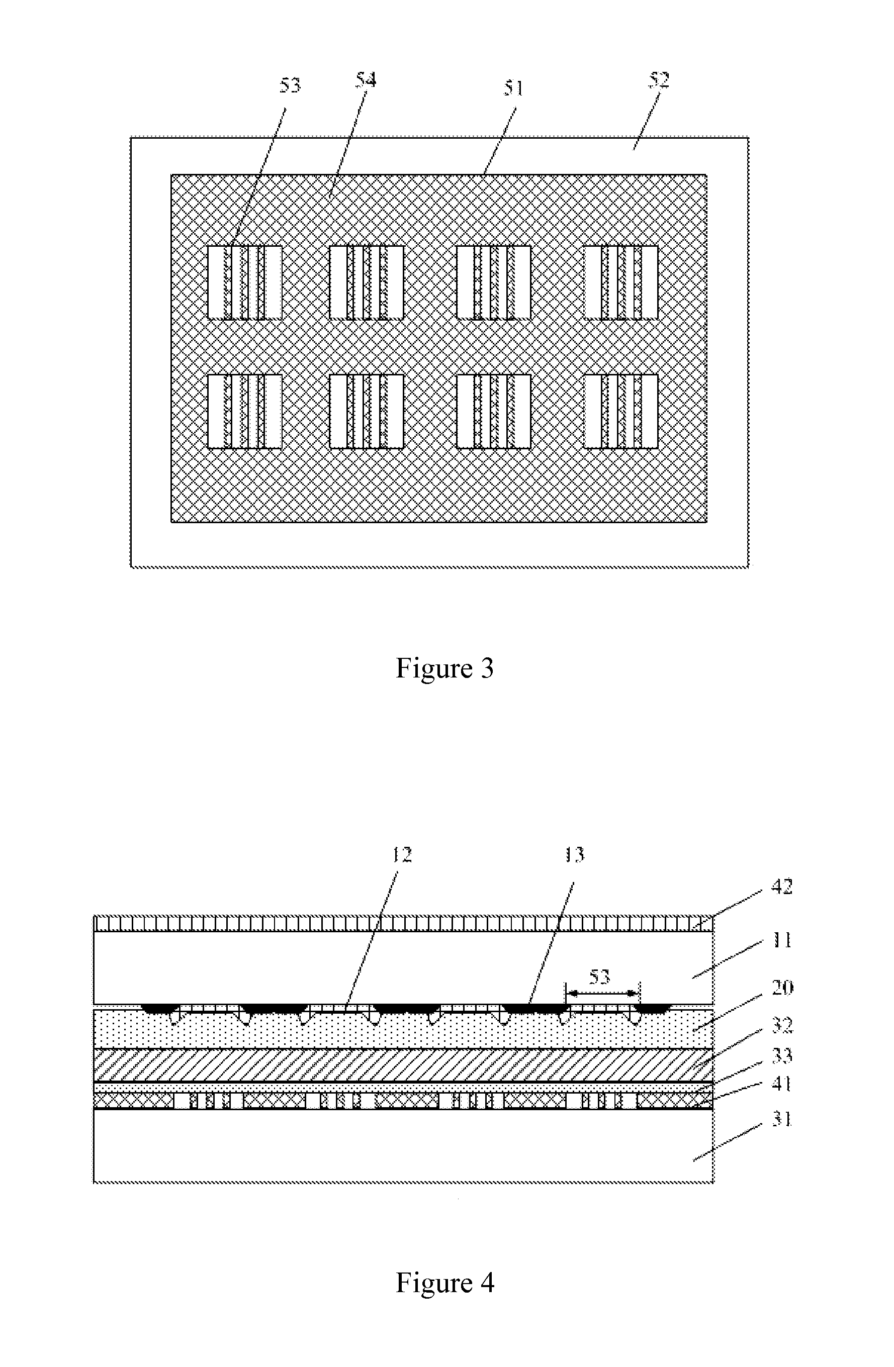
[0065]As shown in FIG. 3, the display panel comprises an active area 51 (AA for short) and an inactive area 52 surrounding the AA, that is, the AA 51 is surrounded within the inactive area 52; in the meantime, referring to FIG. 2, the area corresponding to the AA 51 in the display panel is provided with a polarizer 41, which is the wire grid polarizer with WG structures in embodiment 1.

[0066]The AA 51 includes multiple subpixel areas 53 arranged at intervals, and the areas corresponding to the subpixel areas 53 in the polarizer 41 are the WG structures, while the other area is a metal thin film structure, that is, the area corresponding to the non-subpixel area 54 is a continuous plate structure. The non-subpixel...

embodiment 3

[0085]The embodiment provides a display panel, in which, compared with embodiment 2, the setting location of the polarizer is different from the setting location of the polarizer in the display panel of embodiment 2. This display panel can lower the light absorption rate effectively, and avoid the peripheral light leakage in the non-subpixel area, achieving a good display effect.

[0086]In the display panel of the embodiment, the polarizer is disposed relatively above the array substrate plate. As shown in FIG. 4, the polarizer 41 is disposed between the TFT array 32 and the second base 31, and an insulating layer 33 is disposed between the polarizer 41 and the TFT array 32. The insulating layer 33 is formed above the polarizer 41 to isolate the polarizer 41 from the TFT array 32, so as to avoid the control functions of the TFT array 32 being affected by the metal forming the polarizer 41. Herein, the TFTs of the TFT array 32 can be a top gate type or a bottom gate type.

[0087]The rest...


PUM

PropertyMeasurementUnit
widthaaaaaaaaaa
thicknessaaaaaaaaaa
temperatureaaaaaaaaaa

Abstract

The invention relates to the display technology field, and particularly to a wire grid polarizer, a manufacturing method thereof, a display panel and a display device. The wire grid polarizer comprises a substrate, in which wire grid structures are arranged at intervals in an array, to allow light to penetrate from the grid pitches thereof, with the other area except the wire grid structures of the substrate being a continuous opaque area. Due to the wire grid polarizer being provided with the wire grid structures arranged at intervals in a array, local light transmitting areas can be formed, and light emergence can be controlled more flexibly. A display panel using the wire grid polarizer can effectively lower the light absorption rate, also avoid peripheral light leakage in a non-subpixel area, and prevent the light leakage of the pixels themselves; correspondingly, a display device using the display panel can improve the light utilization rate, and achieve a good display effect.

Description

TECHNICAL FIELD[0001]The invention relates to the display technical field, and particularly to a wire grid polarizer and a manufacturing method thereof, a display panel and a display device.BACKGROUND OF THE INVENTION[0002]A liquid crystal display (LCD for short) is a kind of flat display devices, with an LCD panel and a backlight source as important components thereof. The LCD is formed by setting a backlight source on one side of an LCD panel to achieve image display.[0003]An LCD panel comprises a color film substrate, an array substrate and a liquid crystal (LC) layer disposed between them, with a backlight source disposed at the side close to the array substrate. To achieve image display, the array substrate is provided with thin film transistors (TFT for short), with the control terminals thereof receiving control signals and display signals respectively, and implementing the on / off control of the TFTs according to the control signals and the display signals, so as to drive the...

Claims


Application Information

Patent Timeline
Patent Type & Authority Applications(United States)
IPC IPC(8): G02F1/1335G02F1/1368H01L27/12G02B5/30
CPCG02F1/133528G02B5/3058G02F2001/133548H01L27/1214G02F1/1368G02F1/133548G02F1/133536G02B5/30
Inventor LIU, KAIRANWU, YANBINGLI, WENBOZHANG, XIANGYAN
Owner BOE TECH GRP CO LTD
Learn More