
Methods of Laser Trace Post Processing and Depaneling of Assembled Printed Circuit

a printed circuit and laser trace technology, applied in the direction of printed circuit parts, laser beam welding apparatus, electrical apparatus, etc., can solve the problems of time-consuming and expensive processing of generic pcba to become pcba for a specific product, time-consuming and complicated coordination of all, and lag time affecting suppliers and businesses

Active Publication Date: 2016-11-17
SMART WAVE TECH
View PDF3 Cites 5 Cited by
  • Summary
  • Abstract
  • Description
  • Claims
  • Application Information

AI Technical Summary

Benefits of technology

This patent describes a machine that uses two lasers to make changes to a panel of computer circuit boards. The first laser is used to create separate units for each circuit board in the panel, and the second laser is used to remove the panel from its current state. The process allows for quick and efficient changes to the circuit boards, with no delay between the individualization and depanelling stages. In summary, the machine helps streamline the manufacturing process for computer circuit boards.

Problems solved by technology

As such, the processing of a generic PCBa to become a PCBa for a specific product can be time-consuming and expensive.
As is known, any lag time can be detrimental to suppliers and businesses in getting their product to the market as quickly as possible to meet changing consumer demands.
As is well understood, it can be time-consuming and complicated to coordinate all the necessary post-processing steps and then transport the product overseas to the market destination.

Method used


Image

  • Methods of Laser Trace Post Processing and Depaneling of Assembled Printed Circuit
  • Methods of Laser Trace Post Processing and Depaneling of Assembled Printed Circuit
  • Methods of Laser Trace Post Processing and Depaneling of Assembled Printed Circuit

Examples


Embodiment Construction

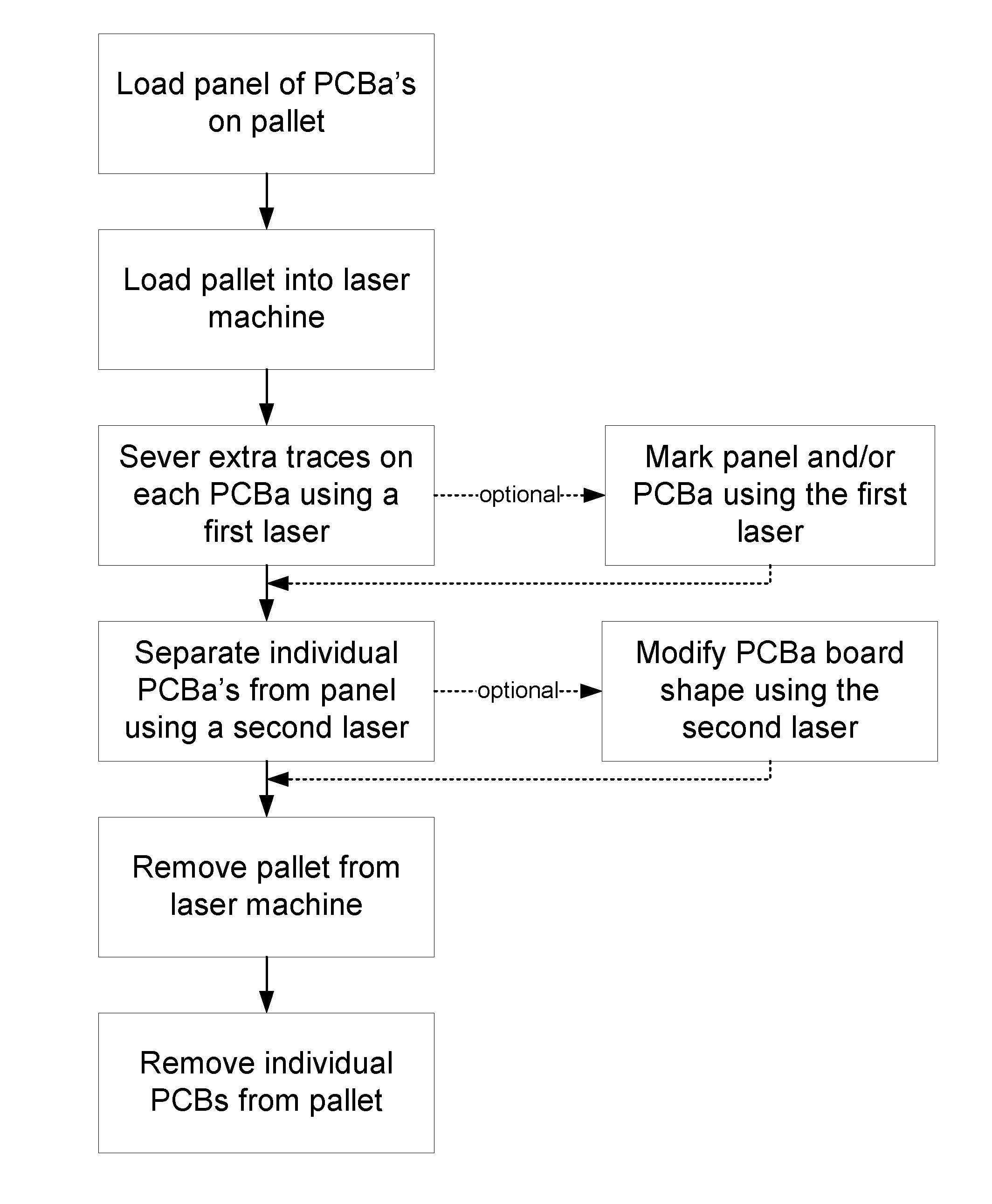
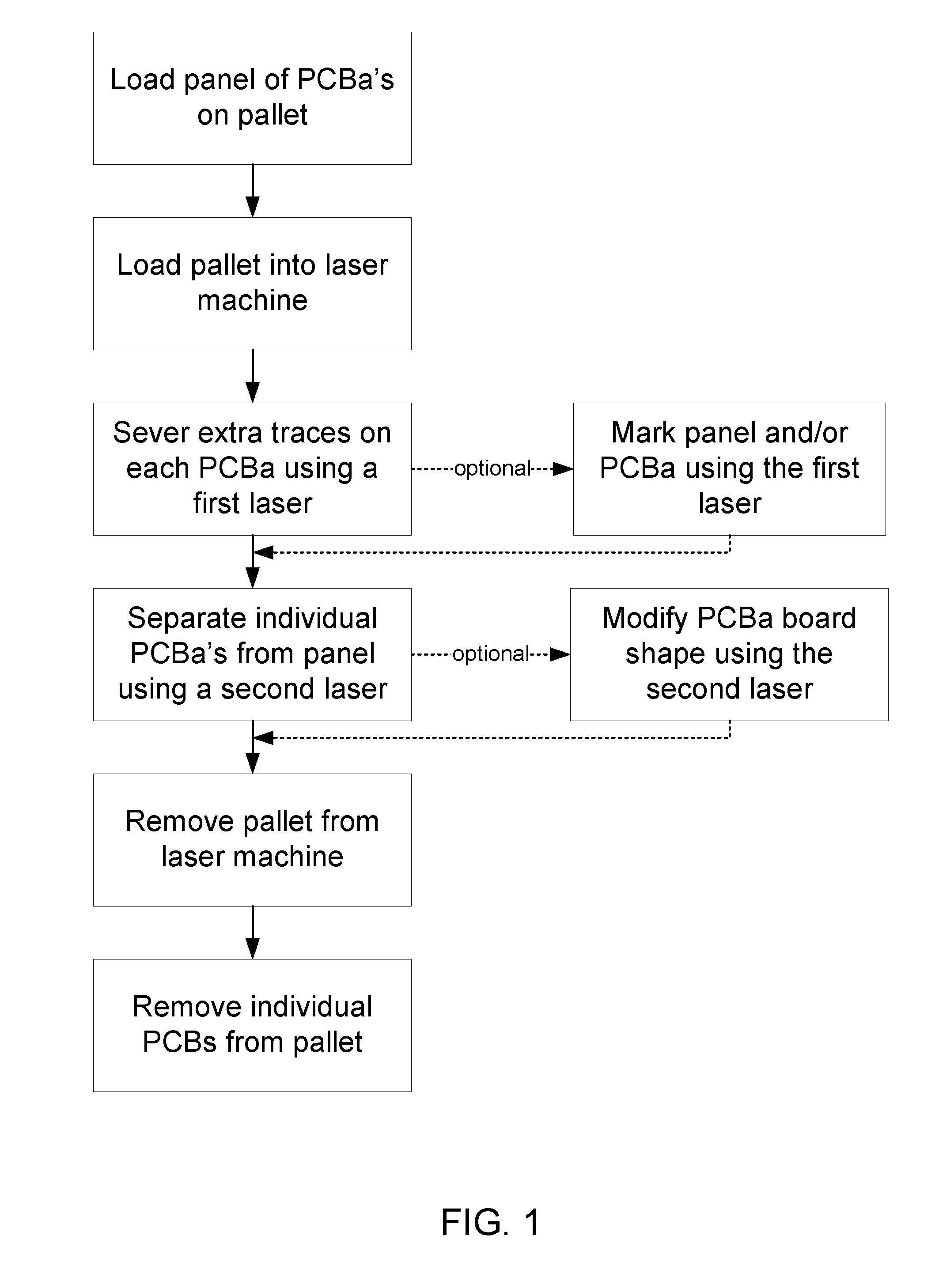
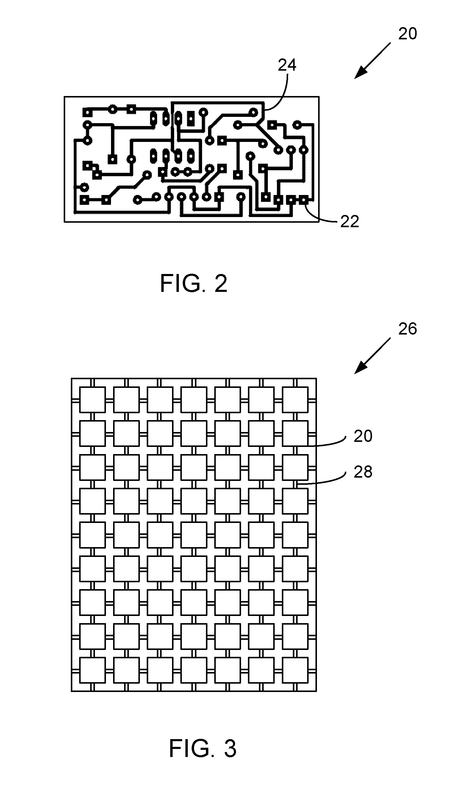
[0025]With reference to FIG. 1, a process for individualizing PCBa's for specific SKUs and depaneling a PCBa panel into individual PCBa's in substantially one step using a single machine is described. The process is designed to efficiently and effectively process a PCBa panel in order to individualize each PCBa and depanel the panel. A typical and individual PCBa 20 is shown in FIG. 2, wherein the PCBa contains a number of electrical components 22 such as various capacitors, resistors, microprocessors, etc., as well as a number of signal traces 24. In the context of the invention, the PCBa 20 can potentially be integrated into a number of different products having different functionalities wherein prior to assembly into a specific product, the PCBa's functionality is altered to be product specific. In other words, various components of the PCBa are common to a number of different SKUs such that the PCBa includes extra signal traces that link the components that until severed, do not...


PUM

PropertyMeasurementUnit
wavelengthaaaaaaaaaa
power capacityaaaaaaaaaa
wavelengthaaaaaaaaaa

Abstract

A method for processing a PCBa panel to individualize the PCBa's on the PCBa panel and depanel the PCBa panel in substantially one step is described. The PCBa panel initially comprises a number of PCBa's having components and traces common to a number of different product SKUs. During processing, the PCBa panel is loaded into a machine containing a first and second laser. The first laser severs extra traces on each PCBa to individualize the PCBa's for specific SKUs and the second laser cuts the links between each PCBa, thereby depaneling the PCBa panel.

Description

FIELD OF THE INVENTION[0001]The invention relates to a method for post processing an assembled printed circuit board (PCBa) panel by individualizing the PCB and depaneling the PCBa panel using two different lasers.BACKGROUND OF THE INVENTION[0002]An assembled printed circuit board (PCBa) is used to mechanically support and electrically connect electronic components using conductive pathways, tracks or signal traces etched from copper sheets that are laminated onto a non-conductive substrate. A PCBa also generally includes various circuit elements such as capacitors, resistors, processors or other active devices that have been manufactured into the actual substrate of the board. Today, PCBa's are used in virtually all but the simplest commercially produced electronic devices.[0003]When products are manufactured, specific products are generally provided with unique identifiers, commonly referred to as stock keeping units (SKUs) that are used as a means of identifying a specific produc...

Claims


Application Information

Patent Timeline
Patent Type & Authority Applications(United States)
IPC IPC(8): H05K3/00B23K26/351B23K26/38H05K1/02
CPCH05K3/0052H05K1/0292H05K3/0097H05K1/0269B23K2201/42B23K26/38H05K2201/09936H05K2203/108B23K26/351B23K2101/42H05K3/26H05K2203/081H05K2203/171H05K2203/175H05K2203/178
Inventor MCMULLEN, SCOTT ARTHURZOSIMADIS, PETER
Owner SMART WAVE TECH
Learn More