Imaging device, method for driving imaging device, and electronic device
a technology of imaging device and electronic device, which is applied in the direction of radio frequency controlled devices, television systems, transistors, etc., can solve the problems of difficult to reduce the variation in electrical characteristics, the difficulty of a transistor manufacturing process, and the length of total imaging time, etc., to achieve high sensitivity, wide dynamic range, and high quality imaging data
- Summary
- Abstract
- Description
- Claims
- Application Information
AI Technical Summary
Benefits of technology
Problems solved by technology
Method used
Image
Examples
embodiment 1
[0084]In this embodiment, an imaging device that is one embodiment of the present invention is described with reference to drawings.
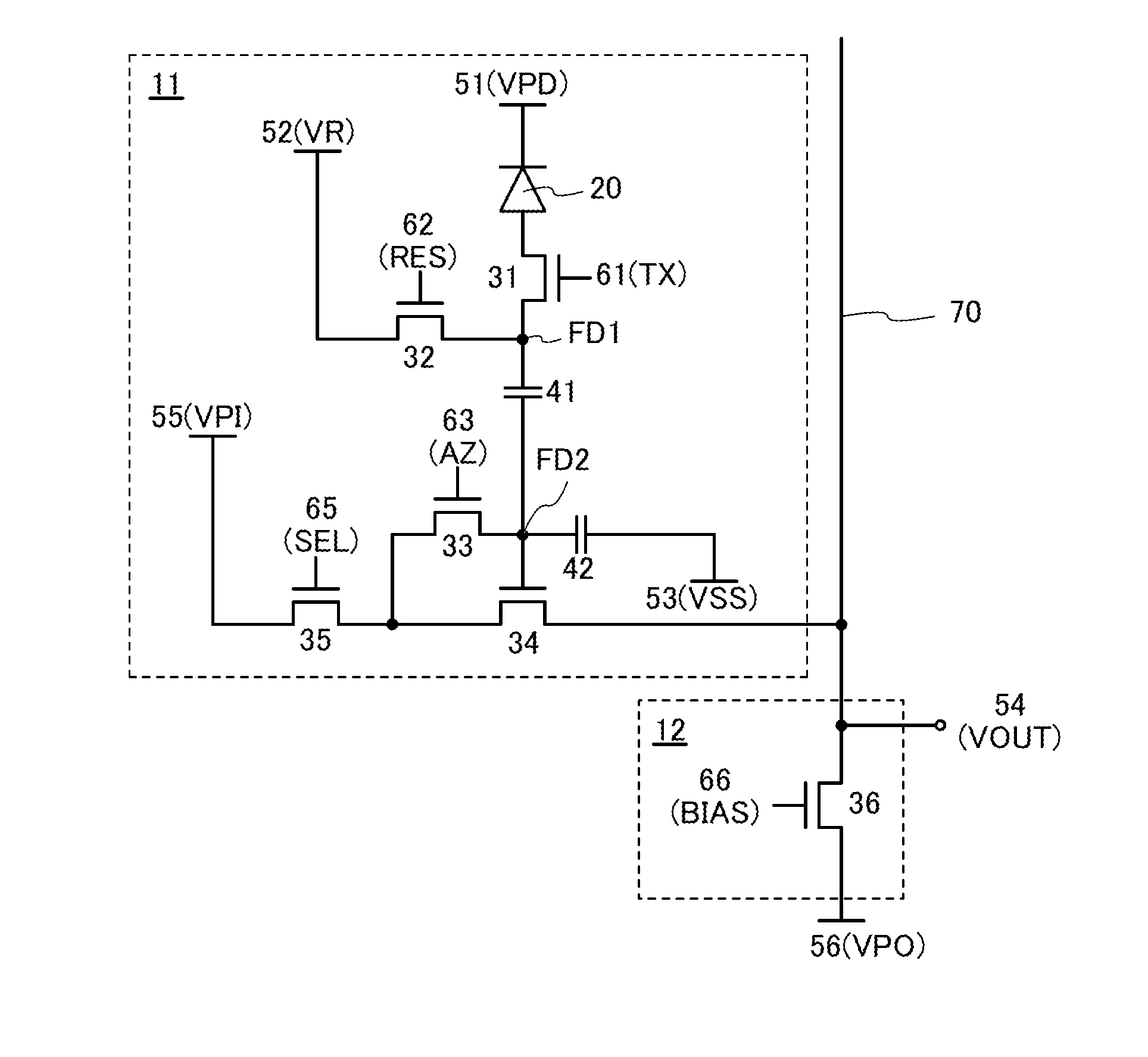
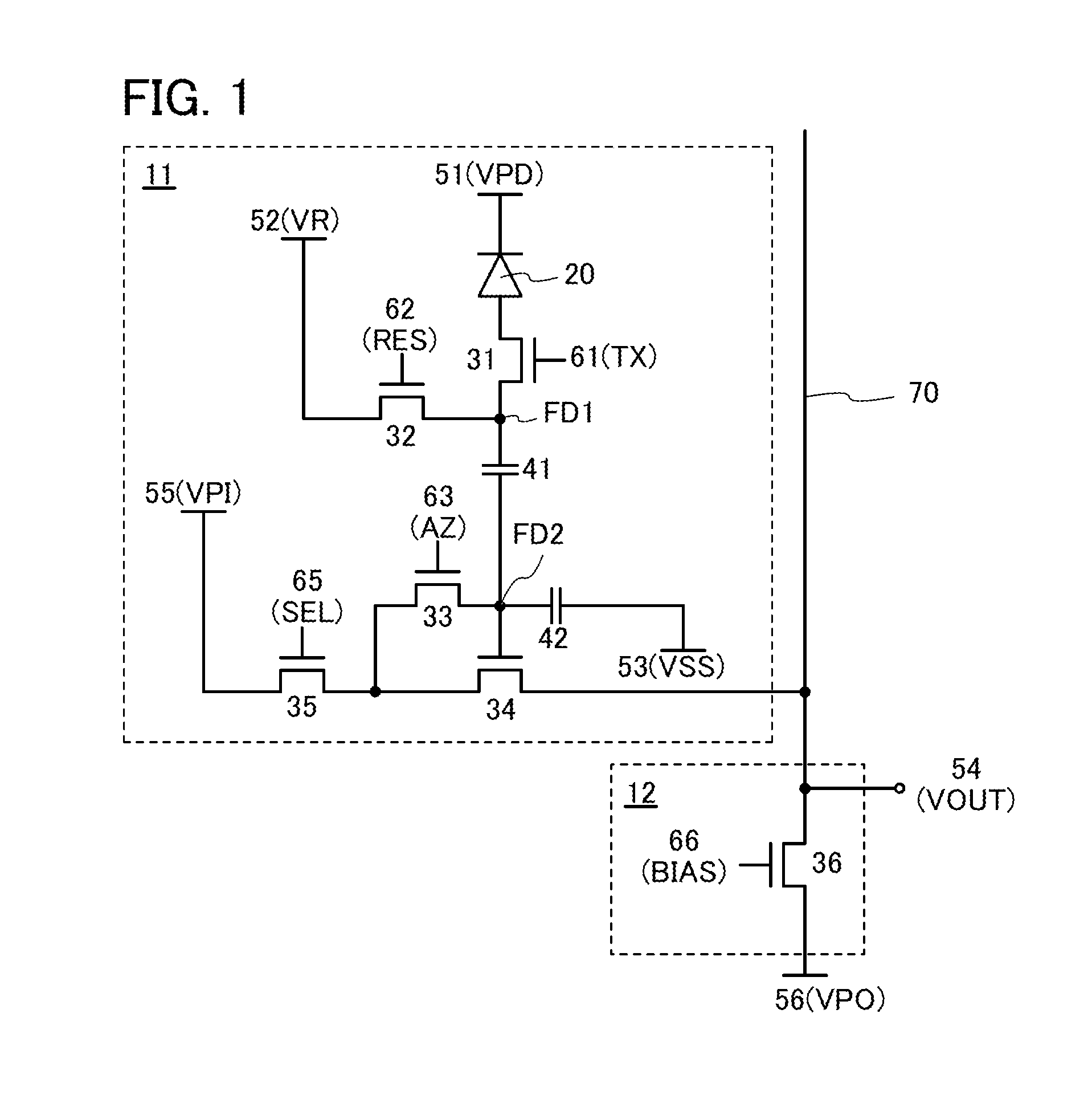
[0085]An imaging device of one embodiment of the present invention includes a pixel circuit capable of compensating variation in the threshold voltage of transistors that function as source follower amplifier transistors in pixels of the imaging device that outputs signal charge (data) by the source followers.
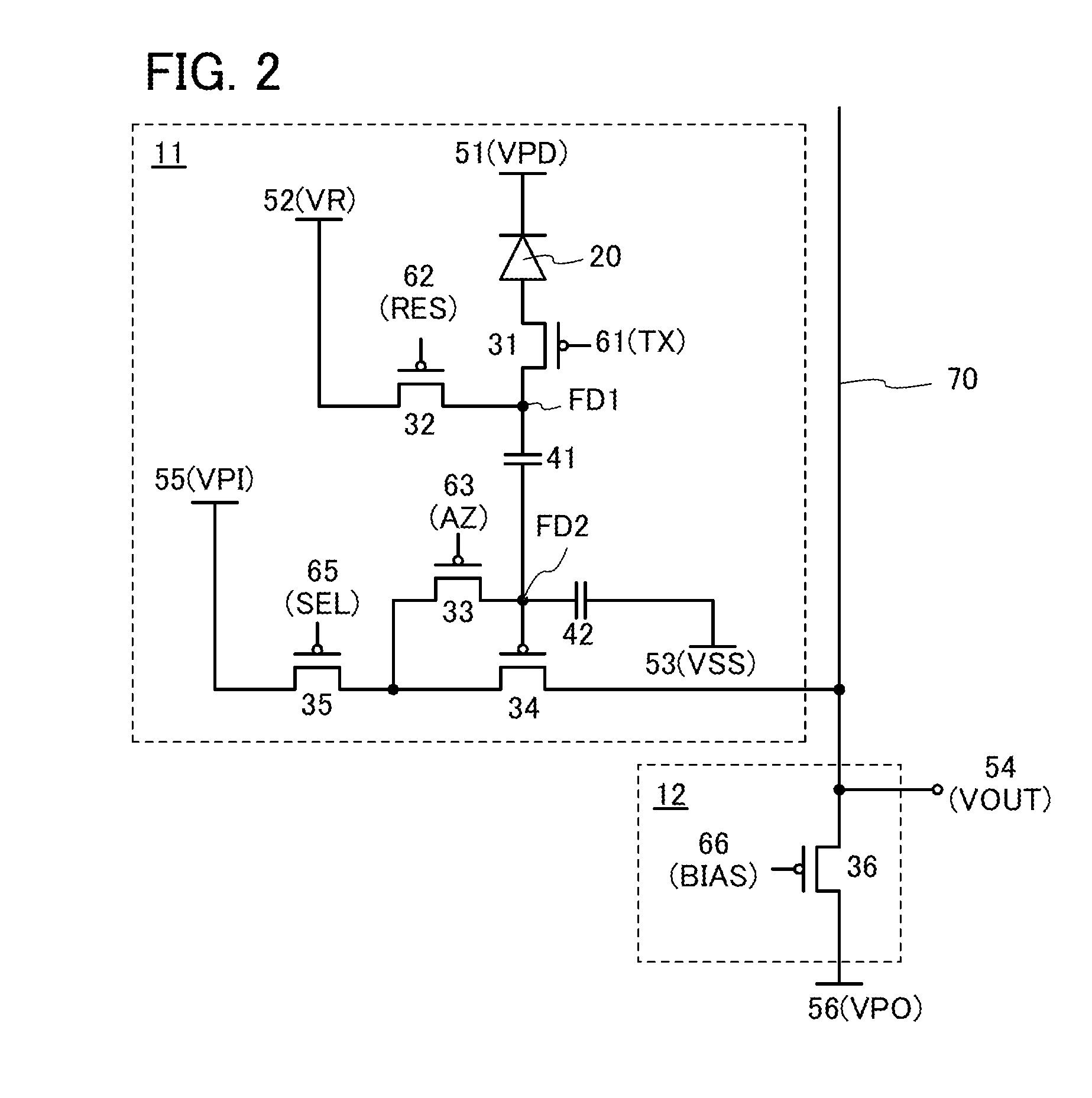
[0086]FIG. 1 is a circuit diagram of a circuit 11 capable of functioning as a pixel circuit and a circuit 12 capable of functioning as an output circuit, included in an imaging device in one embodiment of the present invention. In FIG. 1 and the like, transistors are n-ch transistors; however, one embodiment of the present invention is not limited thereto. The transistors may be p-ch transistors as illustrated in FIG. 2 by reversing the magnitude relationship of a potential. Alternatively, some of the n-ch transistors may be replaced with p-ch tran...
embodiment 2
[0142]In this embodiment, an example of a driving method of a pixel circuit that is different from that in Embodiment 1 is described.
[0143]The pixel circuit described in Embodiment 1 can perform first operation and second operation. In the first operation, the compensation of the threshold voltage “Vth” of the transistor 34 and imaging of an initial frame can be performed. In the second operation, imaging of a difference detection frame can be performed and data indicating a difference (difference data) between the initial frame and the difference detection frame can be output. In the second operation, difference data can be output without a comparison process or the like in an external circuit; thus, the pixel circuit can be applied to a low-power security camera or the like.
[0144]Next, the first operation and the second operation of the circuit in FIG. 1 is described with reference to a timing chart in FIG. 14. Note that the first operation is performed until time T8, and the seco...
embodiment 3
[0166]In this embodiment, specific structure examples of the imaging device in one embodiment of the present invention are described below with reference to drawings.
[0167]FIG. 15A is an example of a cross-sectional view of the imaging device in one embodiment of the present invention and illustrates an example of specific connection between the photoelectric conversion element 20 and the transistors 31 and 32 which are included in the circuit 11 inFIG. 1. Note that FIG. 15A does not illustrate the transistors 33 to 35. The imaging device includes a layer 1100 including the transistors 31 to 35 and a layer 1200 including the photoelectric conversion element 20.
[0168]Although the wirings, the electrodes, and conductors 91 are illustrated as independent components in cross-sectional views in this embodiment, some of them are provided as one component in some cases when they are electrically connected to each other. Moreover, the structure in which the gate electrodes, the source elect...
PUM
 Abstract
Description
Claims
Application Information
 - R&D
- Intellectual Property
- Life Sciences
- Materials
- Tech Scout
- Unparalleled Data Quality
- Higher Quality Content
- 60% Fewer Hallucinations
Browse by: Latest US Patents, China's latest patents, Technical Efficacy Thesaurus, Application Domain, Technology Topic, Popular Technical Reports.
© 2025 PatSnap. All rights reserved.Legal|Privacy policy|Modern Slavery Act Transparency Statement|Sitemap|About US| Contact US: help@patsnap.com


