
Space solar cell panel with blocking diodes

a solar cell and diode technology, applied in the field of photovoltaic power devices, can solve the problems of increasing the overall cost of the photovoltaic array or panel, affecting the efficiency of the surface on which the solar cell is mounted, and requiring a large amount of space, so as to achieve the effect of enhancing space utilization

Inactive Publication Date: 2016-07-28
SOLAERO TECH CORP
View PDF4 Cites 16 Cited by
  • Summary
  • Abstract
  • Description
  • Claims
  • Application Information

AI Technical Summary

Benefits of technology

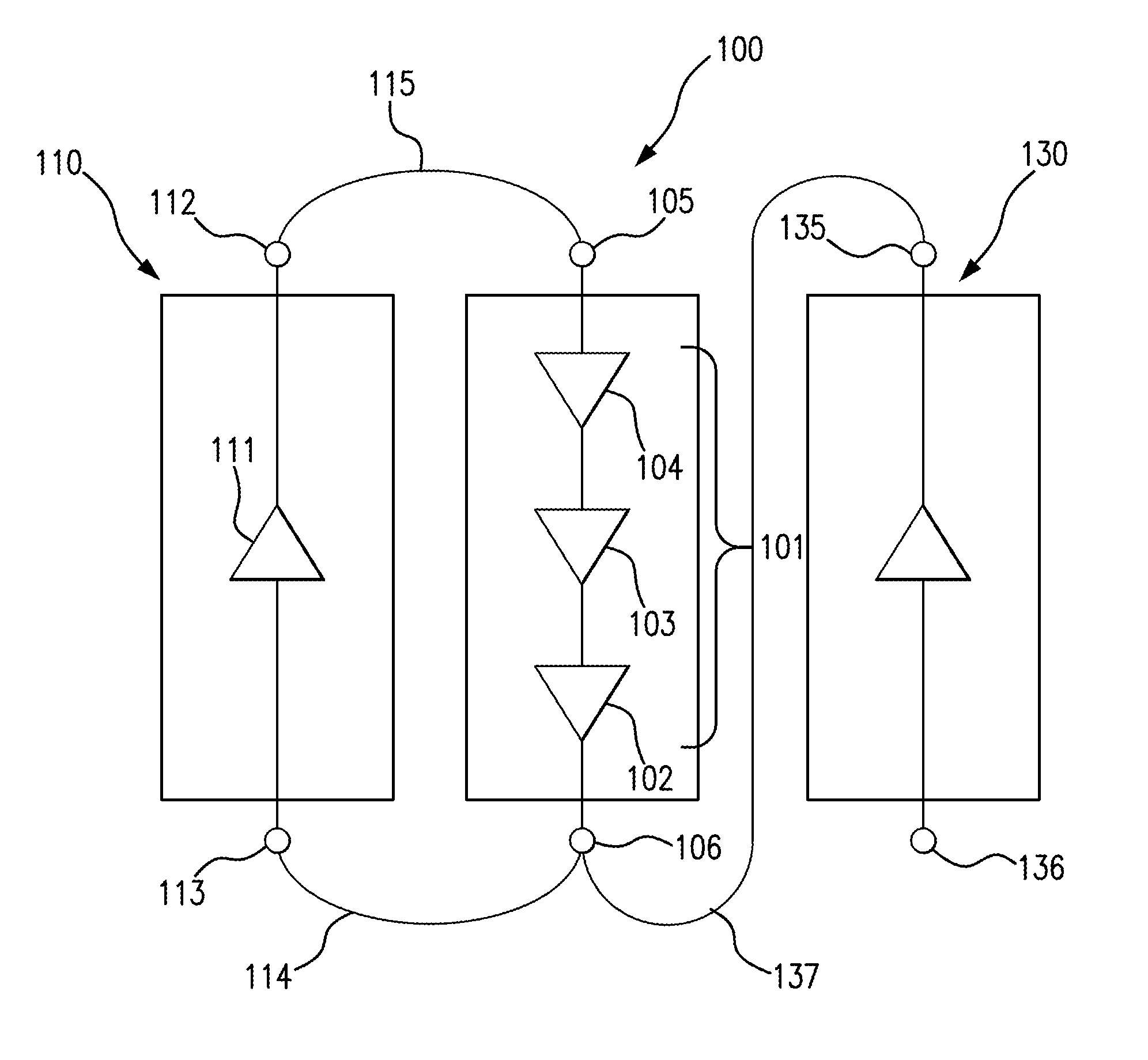
The patent text describes a solar cell assembly that includes a string of solar cells with oblique cut corners. The assembly also includes blocking diodes that are placed in correspondence with the cut corners. This arrangement allows for efficient use of the space between the solar cells and the contact members, such as metal bus bars, which would otherwise be empty. The blocking diodes have a triangular shape that fits snugly into the space left by the cut corners, and can be placed in a space between two adjacent solar cells or in a space between two metallic contact members. The technical effect of this arrangement is improved space utilization in solar cell assemblies.

Problems solved by technology

Compared to silicon, III-V compound semiconductor multijunction devices have greater energy conversion efficiencies and generally more radiation resistance, although they tend to be more complex to manufacture.
Arrays of substantially circular solar cells are known to involve the drawback of inefficient use of the surface on which the solar cells are mounted, due to space that is not covered by the circular solar cells due to the space that is left between adjacent solar cells due to their circular configuration.
However, as explained above, for assembly into a solar array (henceforth, also referred to as a solar cell panel), substantially circular solar cells, which can be produced from substantially circular wafers to minimize waste of wafer material and, therefore, minimize solar cell cost, are often not the best option, due to their low array fill factor, which increases the overall cost of the photovoltaic array or panel and implies an inefficient use of available space.
However, when a single circular wafer is divided into a single rectangle, the wafer utilization is low.
This results in waste.
High efficiency solar cell wafers are often costly to produce.
Thus, the waste that has conventionally been accepted in the art as the price to pay for a high fill factor, that is, the waste that is the result of cutting the rectangular solar cell out of the substantially circular solar cell wafer, can imply a considerable cost.
Some space is wasted at the corners of the solar cells, as the space where the solar cells meet at the cropped corners thereof will not be used for the conversion of solar energy into electrical energy.
However, this wasted space only amounts to a relatively small portion of the entire space occupied by the solar cell array.
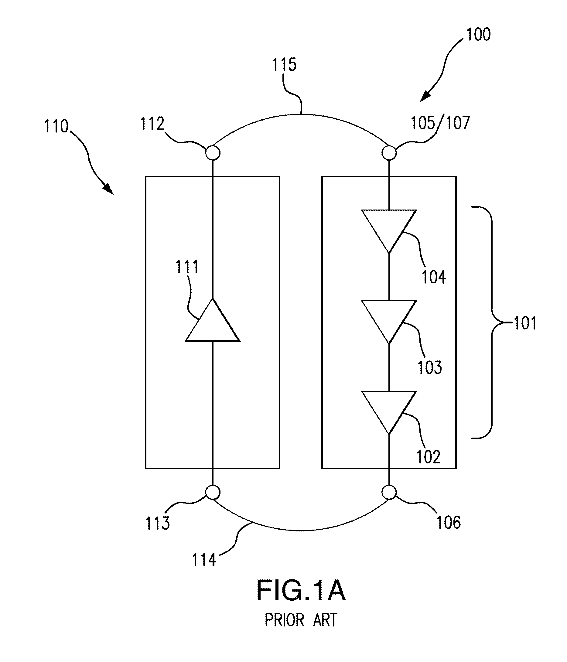
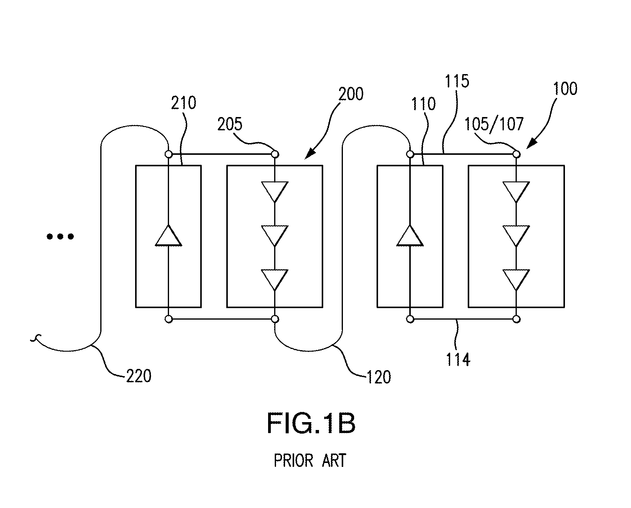
Often, since a panel includes a relatively large amount of solar cells that are connected in series, a relatively substantial blocking diode is required, in terms of size and electrical capacity.
As the blocking diode is generally only present at the end of the string, not much attention has been paid to the way in which it is shaped and connected, as this has not been considered to be of major relevance for the over-all efficiency of the solar cell assembly.

Method used


Image

  • Space solar cell panel with blocking diodes
  • Space solar cell panel with blocking diodes
  • Space solar cell panel with blocking diodes

Examples


Embodiment Construction

[0042]FIG. 2A schematically illustrates how a solar cell 100 with cropped corners can be provided with a bypass diode at one cropped corner, and FIG. 2B schematically illustrates how a bypass diode 110 is arranged in correspondence with one cropped corner and how two blocking diodes 130 and 140 are arranged in correspondence with two of the other cropped corners, in accordance with one embodiment of the disclosure. The two bypass diodes 130 and 140 have substantially triangular shapes, making efficient use of the space at the cropped corners.

[0043]FIGS. 2C, 2D and 2E illustrate how, in accordance with one embodiment of the disclosure, the solar cell can be positioned on a laminar support 140 comprising three layers 141, 142 and 143, to which the solar cell 100 is joined by an adhesive layer 25. The blocking diode 130 is connected to the solar cell 100 by means of a connector 137 which in some embodiments is dispersed in a cut-out region of the adhesive layer 25. The blocking diode 1...


PUM


Abstract

A solar cell assembly or sub-array that comprises a string of series connected solar cells, one of the solar cells being a final solar cell of the string of solar cells. The final solar cell has at least one oblique cut corner. The solar cell assembly further comprises a contact member connected to the final solar cell through a blocking diode, positioned in correspondence with the space provided by the space provided by the oblique cut corner.

Description

REFERENCE TO RELATED APPLICATIONS[0001]This application is related to co-pending U.S. patent application Ser. Nos. 29 / 476,181 and 29 / 476,182 filed Dec. 11, 2013, herein incorporated by reference.BACKGROUND OF THE DISCLOSURE[0002]1. Field of the Disclosure[0003]The disclosure relates to the field of photovoltaic power devices.[0004]2. Description of the Related Art[0005]Solar power from photovoltaic cells, also called solar cells, has been predominantly provided by silicon semiconductor technology. In the past several years, however, high-volume manufacturing of III-V compound semiconductor multijunction solar cells for space applications has accelerated the development of such technology not only for use in space but also for terrestrial solar power applications. Compared to silicon, III-V compound semiconductor multijunction devices have greater energy conversion efficiencies and generally more radiation resistance, although they tend to be more complex to manufacture. Typical comm...

Claims


Application Information

Patent Timeline
IPC IPC(8): H02S40/34H02S40/36H01L31/05
CPCH02S40/34H02S40/36H01L31/0504H01L31/042H01L31/0508H01L31/044Y02E10/50
Inventor CRIST, KEVIN
Owner SOLAERO TECH CORP
Learn More