
Photodetector with Interdigitated Nanoelectrode Grating Antenna

a nano-electrode grating and photodetector technology, applied in the field of photodetectors, can solve the problems of reducing the quantum efficiency of the photodetector, limiting the utility of the device, and disadvantageous to the electro-optic response of the photodetector, so as to enhance the photodetection scheme, enhance the absorption in the active layer, and minimize the distance between electron hole creation and current collection

Inactive Publication Date: 2016-06-16
SANDIA
View PDF4 Cites 35 Cited by
  • Summary
  • Abstract
  • Description
  • Claims
  • Application Information

AI Technical Summary

Benefits of technology

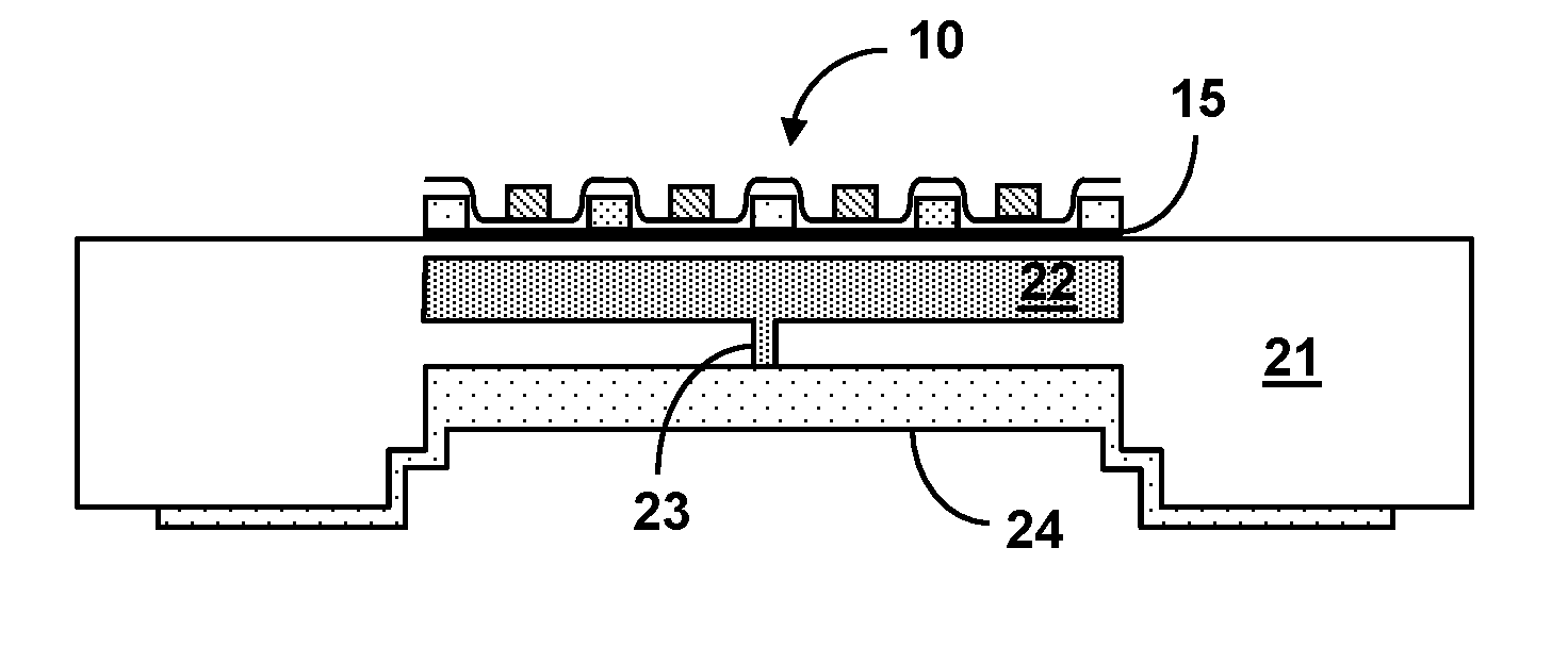
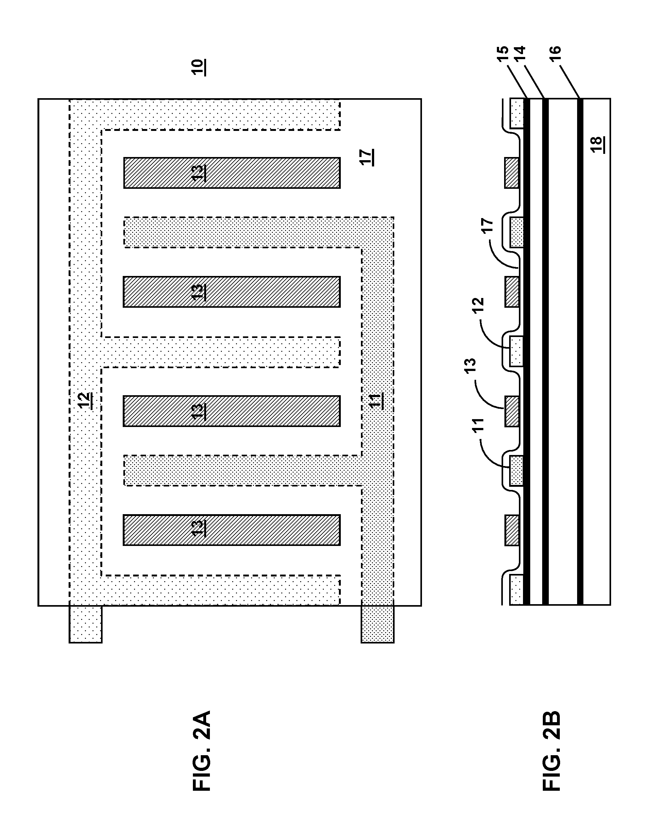
The present invention is an electrode structure that acts as both an absorption-enhancing nanoantenna and a current collector, improving photodetection using two-dimensional semiconducting materials. The structure includes interdigitated source, drain, and gate electrodes that resonantly couple with incident light, resulting in enhanced absorption in the active layer. The structure is designed for enhanced absorption and minimized electron-hole creation and current collection, improving efficiency and sensitivity of photodetection. The technical effect is a more efficient and sensitive photodetector.

Problems solved by technology

Despite the promise of photodetection using an active layer of two-dimensional materials, the state of the art suffers from two major deficiencies: (1) lack of absorption stemming from the atomic thinness of the active material, and (2) absorption enhancing mechanisms limit the utility of the device.
At times, their presence may even increase the distance between the creation of electron-hole pairs and their collection, thereby reducing the quantum efficiency of the photodetector.
Taken together, it is therefore apparent that while nanoantennas make absorption within a two-dimensional material strong enough as to make the device tractable, their presence is oftentimes disadvantageous to the electro-optic response of the photodetector.

Method used


Image

  • Photodetector with Interdigitated Nanoelectrode Grating Antenna
  • Photodetector with Interdigitated Nanoelectrode Grating Antenna
  • Photodetector with Interdigitated Nanoelectrode Grating Antenna

Examples


Embodiment Construction

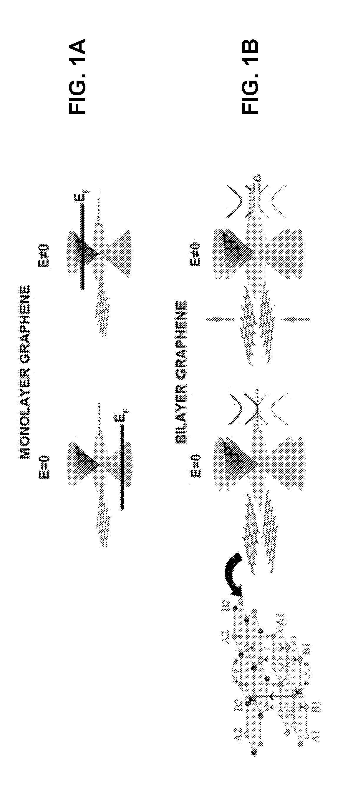
[0018]Monolayer graphene (MLG) is a semi-metal for which at typical pixel sizes it is impossible to create a bandgap. Thus, while previous work has demonstrated MLG's promise as an ultrafast and efficient photodetector, the material's nearly constant broadband response effectively removes any possibility for its use as a filter-less multispectral detector. See F. Xia et. al., Nature Nanotechnology 4, 839 (2009); F. Xia et al., Nano Letters 9, 1039 (2009); and R. R. Nair et al., Science 320, 1308 (2008). MLG's lack of bandgap arises due to its unique electronic structure characterized by two cones that intersect at the Dirac point, which is typically near the Fermi energy (EF), as shown in FIG. 1A. Upon application of a transverse electric field (i.e., E≠0), only the Fermi energy changes and no bandgap forms. Bilayer graphene, on the other hand, has four distinct bands that arise due to the sublattice that is created by the inequivalent sites (A1 vs. A2 and B1 vs. B2 in FIG. 1B) betw...


PUM


Abstract

An interdigitated nanoelectrode grating functions both as an absorption-enhancing sub-wavelength antenna and to minimize the distance between electron-hole creation and current collection so as to enhance photodetection schemes based upon active layers comprising two-dimensional semiconducting materials.

Description

CROSS-REFERENCE TO RELATED APPLICATION[0001]This application is a continuation-in-part of U.S. application Ser. No. 14 / 056,023, filed Oct. 17, 2013, which claims the benefit of U.S. Provisional Application No. 61 / 732,667, filed Dec. 3, 2012, both of which are incorporated herein by reference. This application also claims the benefit of U.S. Provisional Application No. 62 / 114,146, filed Feb. 10, 2015, which is incorporated herein by reference.STATEMENT OF GOVERNMENT INTEREST[0002]This invention was made with Government support under contract no. DE-AC04-94AL85000 awarded by the U. S. Department of Energy to Sandia Corporation. The Government has certain rights in the invention.FIELD OF THE INVENTION[0003]The present invention relates to photodetectors and, in particular, to a photodetector with interdigitated nanoelectrode grating antenna.BACKGROUND OF THE INVENTION[0004]Typical infrared sensor materials are composed of complex semiconductors, such as HgCdTe (MCT) and InGaAs, that ar...

Claims


Application Information

Patent Timeline
Patent Type & Authority Applications(United States)
IPC IPC(8): H01L31/113H01L31/0232
CPCH01L31/02327H01L31/1136H01L31/0232
Inventor BEECHEM, III, THOMAS EDWINHOWELL, STEPHEN W.PETERS, DAVID W.DAVIDS, PAULSHANER, ERIC A.
Owner SANDIA
Learn More