Display Device and Driving Method Thereof
a display device and driving method technology, applied in the direction of electric digital data processing, instruments, computing, etc., can solve the problems of increasing the correction period, difficult to perform external correction in parallel with the display operation of the display device, and unintentional changes of the display, so as to reduce adverse effects, suppress uneven display, and reduce adverse effects
- Summary
- Abstract
- Description
- Claims
- Application Information
AI Technical Summary
Benefits of technology
Problems solved by technology
Method used
Image
Examples
embodiment 1
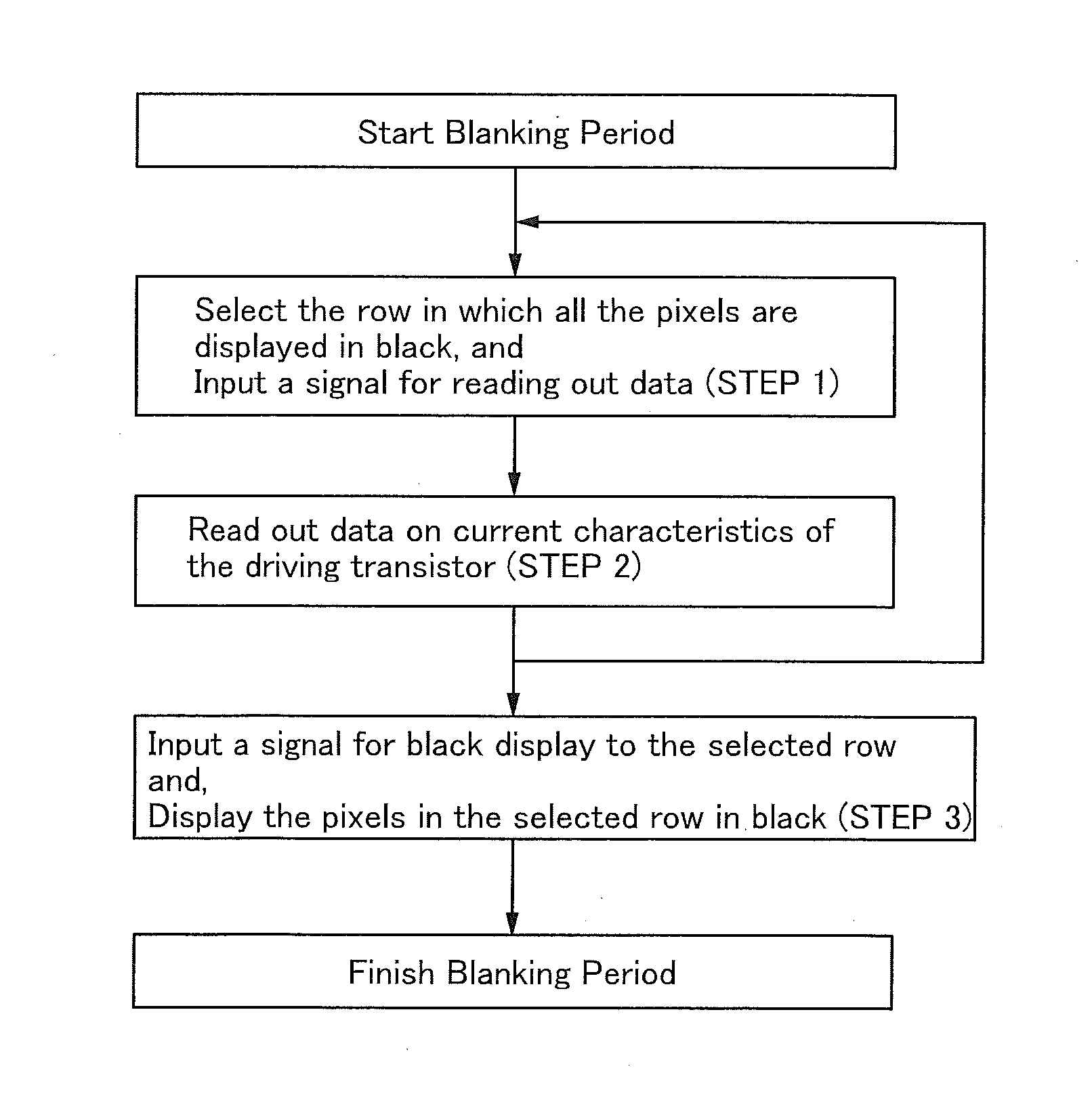
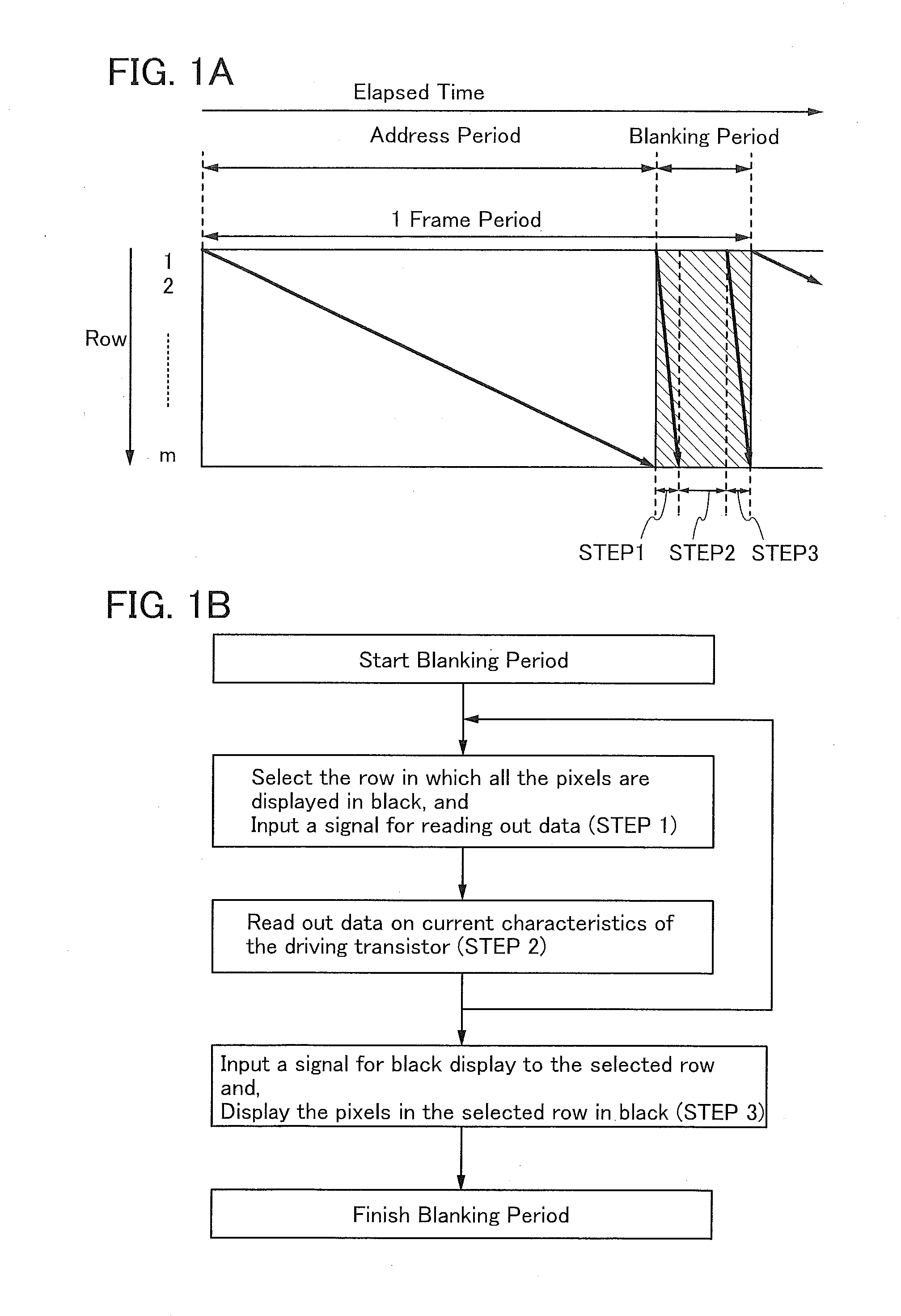
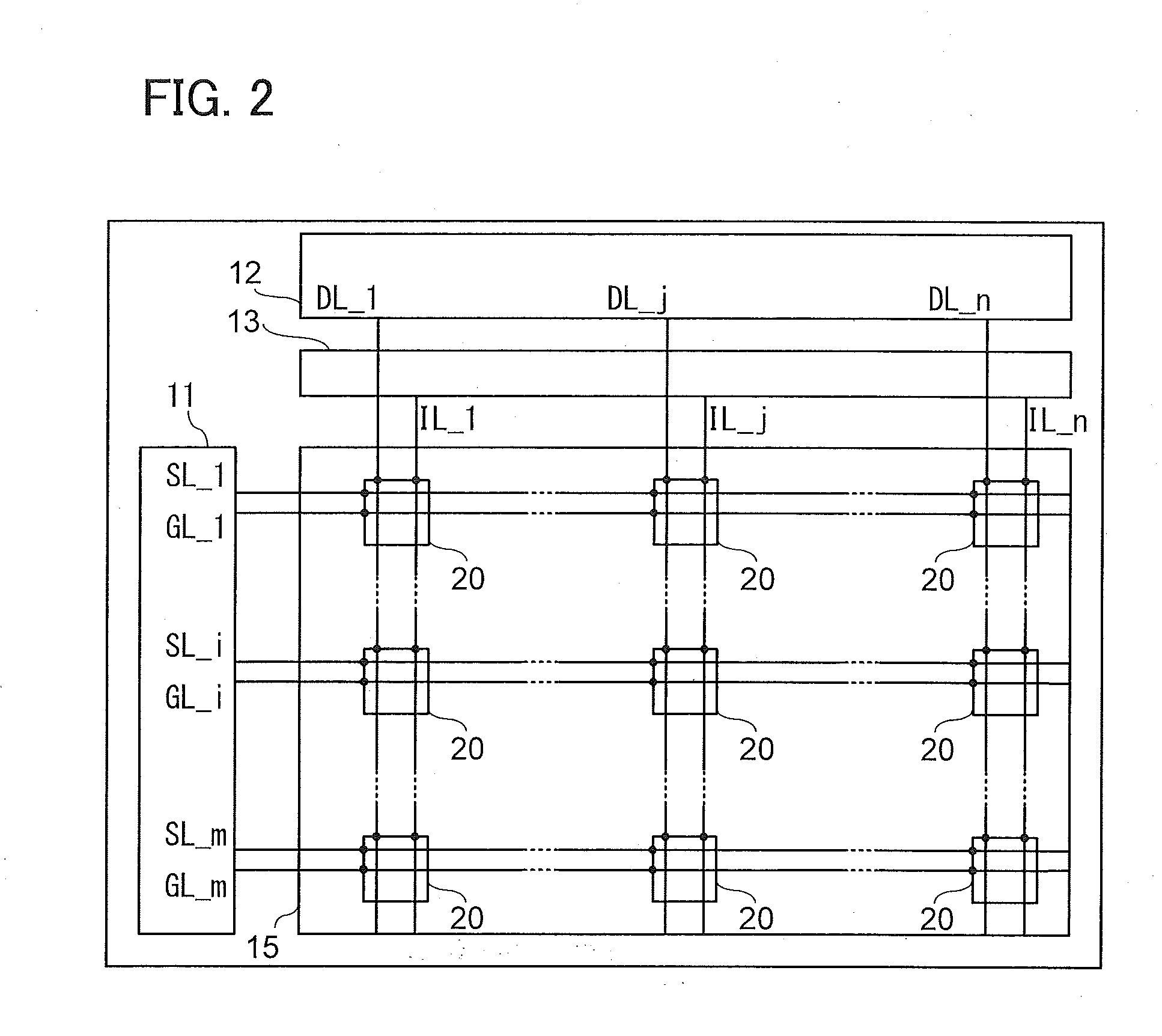
[0072]In this embodiment, a structure of a display device according to one embodiment of the disclosed invention and a driving method thereof will be described with reference to FIGS. 1A and 1B, FIG. 2, FIG. 3, FIG. 4, FIG. 5, FIG. 6, FIG. 7, FIGS. 8A and 8B, FIGS. 9A to 9C, FIG. 10, and FIGS. 11A and 11B.
[0073]FIG. 1A is a timing chart illustrating a driving method of a display device according to one embodiment of the disclosed invention. In the timing chart in FIG. 1A, the horizontal direction indicates elapsed time and the vertical direction indicates the row on which scanning is performed.
[0074]The display device of this embodiment includes a plurality of pixels arranged in a matrix with in rows and n columns (m and n are each an integer greater than or equal to 2). Furthermore, each pixel includes a light-emitting element and a transistor which supplies current to the light-emitting element (hereinafter also referred to as a driving transistor). Furthermore, the display device...
embodiment 2
Modification Example 1 of Display Device
[0177]In this embodiment, a structure of a display device and a driving method thereof which are different from those described in Embodiment 1 are described with reference to FIG. 12 and FIGS. 13A to 13C.
[0178]FIG. 12 shows a pixel structure of the display device of this embodiment. The display device of this embodiment includes, as in the display device in FIG. 2, the pixel portion 15 including (m×n) pixels 50, a variety of peripheral circuits, and a variety of wirings. The same numerals and symbols are used for the peripheral circuits and the wirings.
[0179]Because the pixel structure is different from that in Embodiment 1, the structures of the peripheral circuit and the wiring are partly different from those in FIG. 2. Specifically, the different points are that the wiring IL extends in the row direction and the circuit portion 13 is electrically connected to the wiring DL. In that case, as shown in FIG. 4, switches may be provided so that...
embodiment 3
Modification Example 2 of Display Device
[0229]In this embodiment, a structure of a display device and a driving method thereof which are different from those described in Embodiment 1 are described with reference to FIG. 16 and FIG. 17.
[0230]FIG. 16 shows a pixel structure of the display device of this embodiment. The display device of this embodiment includes, as in the display device in FIG. 2, the pixel portion 15 including (m×n) pixels 70, a variety of peripheral circuits, and a variety of wirings. The same numerals and symbols are used for the peripheral circuits and the wirings.
[0231]FIG. 16 shows a structure of a pixel 70_(i,j) in the i-th row and the j-th column (i is an integer greater than or equal to 1 and less than or equal to m and j is an integer greater than or equal to 1 and less than or equal to n). The pixel 70_(i, j) includes a transistor 71, a p-channel transistor 72, a transistor 73, a light-emitting element 74, and a capacitor 75. Note that these elements inclu...
PUM
 Abstract
Description
Claims
Application Information
 - R&D
- Intellectual Property
- Life Sciences
- Materials
- Tech Scout
- Unparalleled Data Quality
- Higher Quality Content
- 60% Fewer Hallucinations
Browse by: Latest US Patents, China's latest patents, Technical Efficacy Thesaurus, Application Domain, Technology Topic, Popular Technical Reports.
© 2025 PatSnap. All rights reserved.Legal|Privacy policy|Modern Slavery Act Transparency Statement|Sitemap|About US| Contact US: help@patsnap.com


