Light source device for reflective microdisplay panel
a technology of light source device and reflective microdisplay panel, which is applied in the direction of fixed installation, lighting and heating apparatus, instruments, etc., can solve the problems of non-uniformity of lcos panel, size mismatch, and inability to adjust the size of the conventional led package according to the various sizes of the lcos panel, so as to improve the uniformity and contrast of the reflective microdisplay panel
- Summary
- Abstract
- Description
- Claims
- Application Information
AI Technical Summary
Benefits of technology
Problems solved by technology
Method used
Image

Examples
first embodiment
[0019]Please refer to FIG. 3. FIG. 3 shows a simplified diagram of a light source device 300 for a reflective microdisplay panel 310 in accordance with the present invention, wherein the reflective microdisplay panel 310 can be a liquid crystal on a silicon (LCOS) panel, a DMD panel, or an epaper panel. The light source device 300 comprises a first light bar 320 disposed on a first side of the reflective microdisplay panel 310. The first light bar 320 comprises: a substrate 330, a plurality of micro LED units 340, and a controlling unit 350, wherein the substrate 330 can be a silicon substrate, and the size of the first light bar 320 can be adjusted according to the size of the reflective microdisplay panel 310. For example, the size of the reflective microdisplay panel 310 can be 0.22 inches, 0.29 inches, 0.35 inches, 0.5 inches, or 0.7 inches, and the size of the first light bar 320 can be adjusted accordingly.
[0020]The micro LED units 340 are formed on the substrate 330, and each...
second embodiment
[0021]Please refer to FIG. 4. FIG. 4 shows a simplified diagram of a light source device 400 for a reflective microdisplay panel 410 in accordance with the present invention. The light source device 400 comprises a first light bar 420 and a second light bar 422, wherein the first light bar 420 is disposed on a first side of the reflective microdisplay panel 410, and the second light bar 422 is disposed on a second side of the reflective microdisplay panel 410.
[0022]The first light bar 420 comprises: a substrate 430, a plurality of micro LED units 440, and a controlling unit 450, wherein the substrate 430 can be a silicon substrate, and the size of the first light bar 420 can be adjusted according to the size of the reflective microdisplay panel 410. The second light bar 422 comprises: a substrate 432, a plurality of micro LED units 442, and a controlling unit 452, wherein the substrate 432 can be a silicon substrate, and the size of the second light bar 422 can be adjusted according...
third embodiment
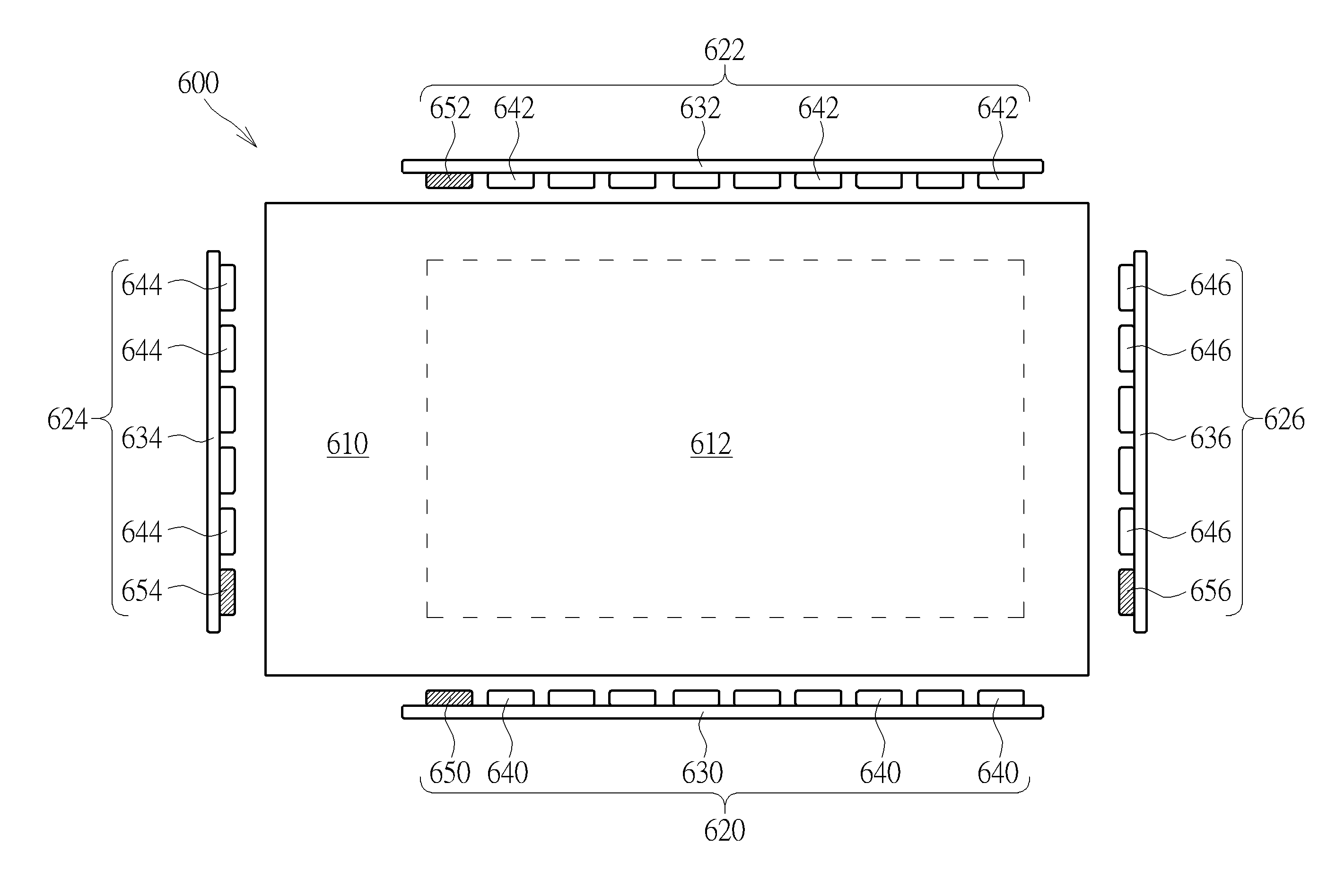
[0025]Please refer to FIG. 5. FIG. 5 shows a simplified diagram of a light source device 500 for a reflective microdisplay panel 510 in accordance with the present invention. The light source device 500 comprises a first light bar 520, a second light bar 522, and a third light bar 524, wherein the first light bar 520 is disposed on a first side of the reflective microdisplay panel 510, and the second light bar 522 is disposed on a second side of the reflective microdisplay panel 510, and the third light bar 524 is disposed on a third side of the reflective microdisplay panel 510.
[0026]The first light bar 520 comprises: a substrate 530, a plurality of micro LED units 540, and a controlling unit 550, wherein the substrate 530 can be a silicon substrate, and the size of the first light bar 520 can be adjusted according to the size of the reflective microdisplay panel 510. The second light bar 522 comprises: a substrate 532, a plurality of micro LED units 542, and a controlling unit 552...
PUM
| Property | Measurement | Unit |
|---|---|---|
| sizes | aaaaa | aaaaa |
| sizes | aaaaa | aaaaa |
| sizes | aaaaa | aaaaa |
Abstract
Description
Claims
Application Information
 - R&D
- Intellectual Property
- Life Sciences
- Materials
- Tech Scout
- Unparalleled Data Quality
- Higher Quality Content
- 60% Fewer Hallucinations
Browse by: Latest US Patents, China's latest patents, Technical Efficacy Thesaurus, Application Domain, Technology Topic, Popular Technical Reports.
© 2025 PatSnap. All rights reserved.Legal|Privacy policy|Modern Slavery Act Transparency Statement|Sitemap|About US| Contact US: help@patsnap.com