
Endpoint determination using individually measured target spectra

a technology of individual measurement and endpoint determination, applied in the direction of lapping machines, program control, instruments, etc., can solve the problems of differences in the time needed to reach the polishing endpoint, electrical shorting, errors in determining the endpoint, etc., and achieve the effect of reducing the inherent complications

Inactive Publication Date: 2016-02-04
GLOBALFOUNDRIES INC +1
View PDF4 Cites 0 Cited by
  • Summary
  • Abstract
  • Description
  • Claims
  • Application Information

AI Technical Summary

Benefits of technology

The patent describes methods for accurately determining when a polishing process is complete on a semiconductor device. This is important because it ensures that the device is properly formed and can be used for its intended purpose. The methods involve measuring the target spectra of the device before and after the polishing process, and using an algorithm to determine the endpoint of the polishing process. This approach reduces complications by measuring the target spectra of each device individually, rather than relying on uncertain or estimated targets. Overall, the patent provides a more reliable and efficient way to measure the processing endpoint of semiconductor devices.

Problems solved by technology

One problem in CMP is determining whether the polishing process is complete, i.e., whether a substrate layer has been planarized to a desired flatness or thickness, or when a desired amount of material has been removed.
On the other hand, under polishing (i.e., removing too little) of a conductive layer leads to electrical shorting.
These variations cause differences in the time needed to reach the polishing endpoint.
In one prior art approach, white light (WL) is used as an alternative endpoint determination method because it is very sensitive.
Since the WL signal is sensitive to minor changes in substrates, the assumed target is not always accurate and, therefore, often leads to mistakes determining the endpoint.

Method used


Image

  • Endpoint determination using individually measured target spectra
  • Endpoint determination using individually measured target spectra
  • Endpoint determination using individually measured target spectra

Examples


Embodiment Construction

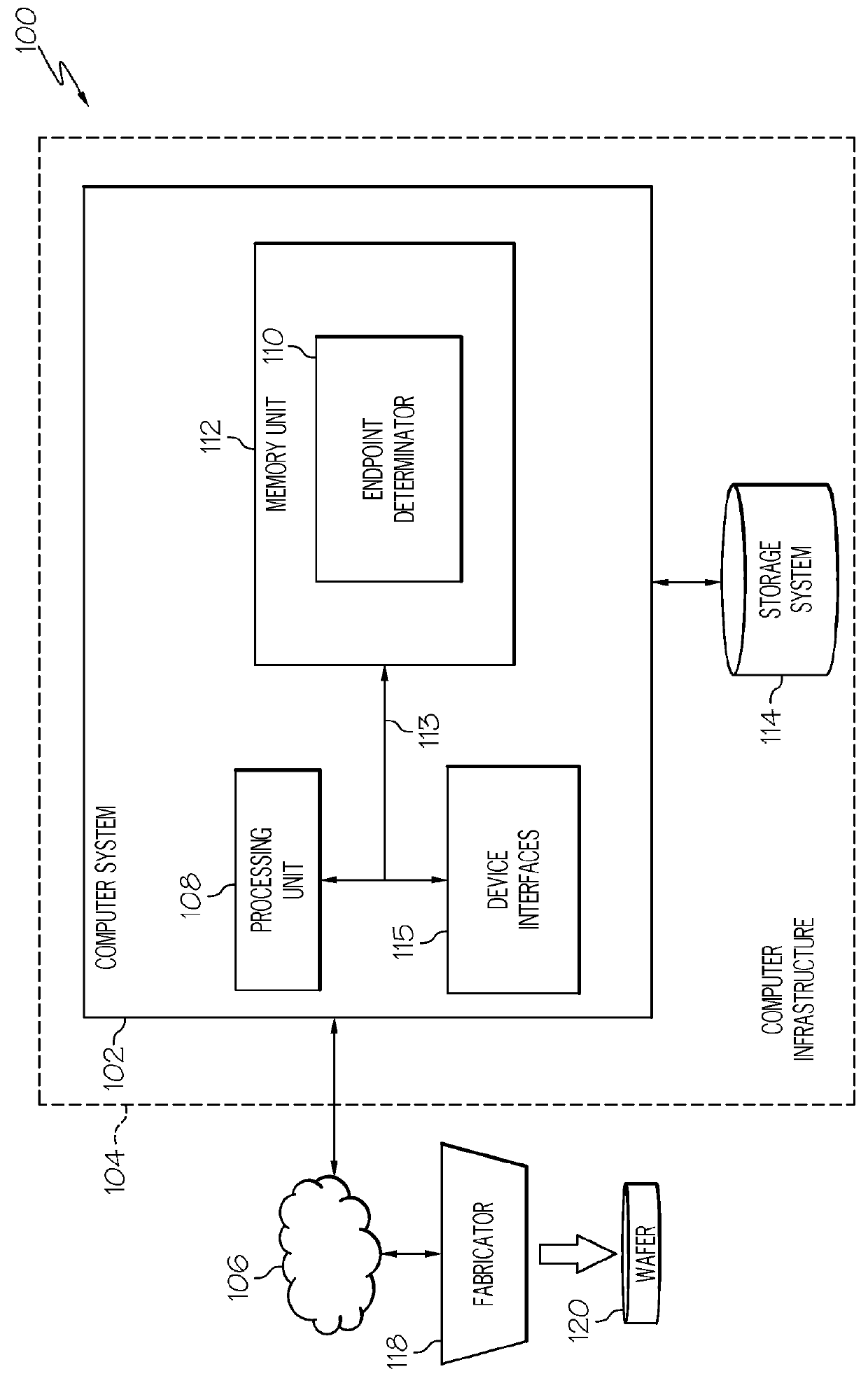
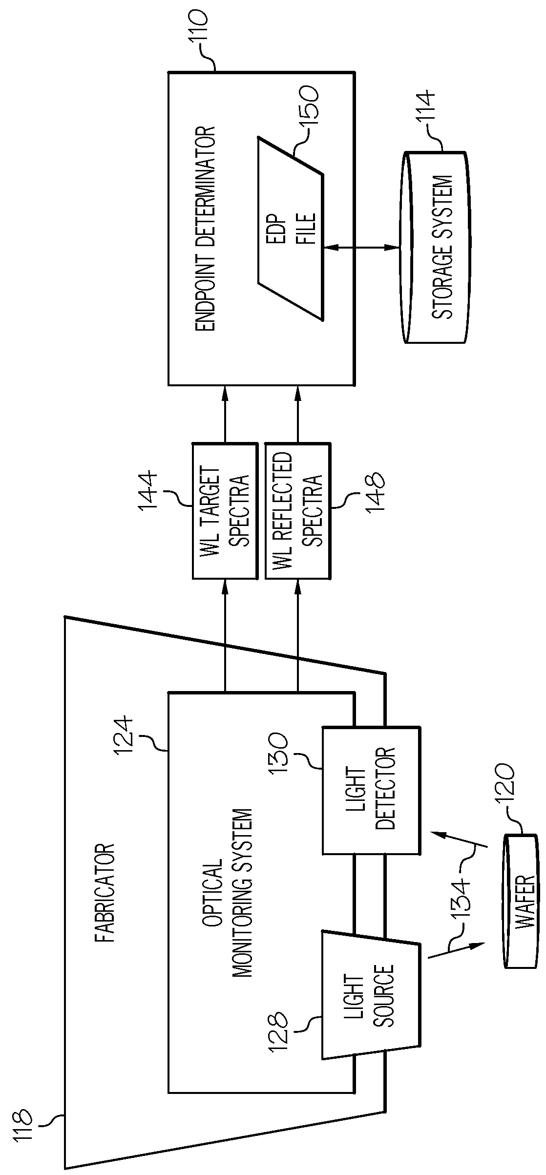
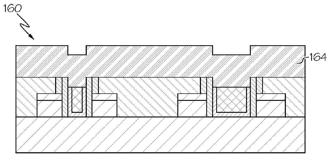
[0021]Exemplary embodiments will now be described more fully herein with reference to the accompanying drawings, in which exemplary embodiments are shown. It will be appreciated that this disclosure may be embodied in many different forms and should not be construed as limited to the exemplary embodiments set forth herein. Rather, these exemplary embodiments are provided so that this disclosure will be thorough and complete and will fully convey the scope of this disclosure to those skilled in the art. The terminology used herein is for the purpose of describing particular embodiments only and is not intended to be limiting of this disclosure. For example, as used herein, the singular forms “a”, “an”, and “the” are intended to include the plural forms as well, unless the context clearly indicates otherwise. Furthermore, the use of the terms “a”, “an”, etc., do not denote a limitation of quantity, but rather denote the presence of at least one of the referenced items. It will be furt...


PUM


Abstract

Disclosed are approaches for determining a processing endpoint using individually measured target spectra. More specifically, one approach includes: measuring a white light (WL) target spectra of a semiconductor device on an individual wafer prior to formation of a polishing / planarization material; inputting the WL target spectra to a WL endpoint algorithm of the semiconductor device following formation of the polishing / planarization material; and determining, using the WL endpoint algorithm, the processing endpoint of the polishing / planarization material of the semiconductor device. In another approach, the endpoint measurement process comprises receiving spectra reflected from the semiconductor device during polishing, and comparing the spectra to the WL target spectra, which is previously stored within a storage device. As such, WL target spectra are measured “as is” (e.g., without simplifications, generalizations, assumptions, etc.) for each wafer to reduce complications inherent with the use of an uncertain and / or estimated target.

Description

BACKGROUND[0001]1. Field of the Invention[0002]This invention relates generally to semiconductor device endpoint determination and, more specifically, to providing individual measured target spectra to improve endpoint determination accuracy.[0003]2. Description of the Related Art[0004]An integrated circuit is typically formed on a substrate by the sequential deposition of conductive, semiconductive, or insulator layers on a silicon wafer. One fabrication step involves depositing a filler layer over a non-planar surface and planarizing the filler layer. For certain applications, the filler layer is planarized until the top surface of a patterned layer is exposed. A conductive filler layer, for example, can be deposited on a patterned insulator layer to fill the trenches or holes in the insulator layer. After planarization, the portions of the conductive layer remaining between the raised pattern of the insulator layer form vias, plugs, and lines that provide conductive paths between...

Claims


Application Information

Patent Timeline
IPC IPC(8): G05B19/418
CPCG05B2219/45031G05B19/418B24B37/013B24B49/12H01L22/12H01L22/26H01L21/31053H01L21/3212
Inventor TSAI, STANSURISETTY, CHARAN V. V. S.
Owner GLOBALFOUNDRIES INC
Learn More