Method of measuring contamination amount of vapor phase growth apparatus, and method of manufacturing epitaxial wafer
a technology of vapor phase growth and contamination amount, which is applied in the testing/measurement of individual semiconductor devices, semiconductor/solid-state devices, instruments, etc., can solve the problems of white spot, contaminated epitaxial wafer, and white spot, and achieve high sensitivity
- Summary
- Abstract
- Description
- Claims
- Application Information
AI Technical Summary
Benefits of technology
Problems solved by technology
Method used
Image

Examples
example 1
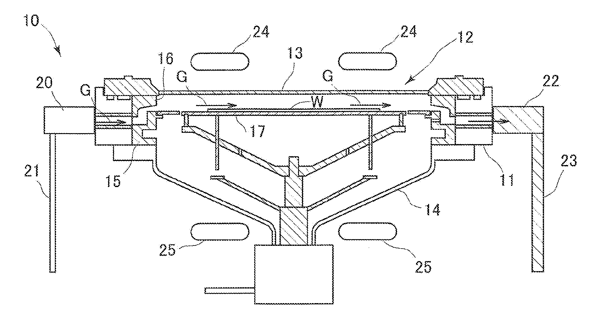
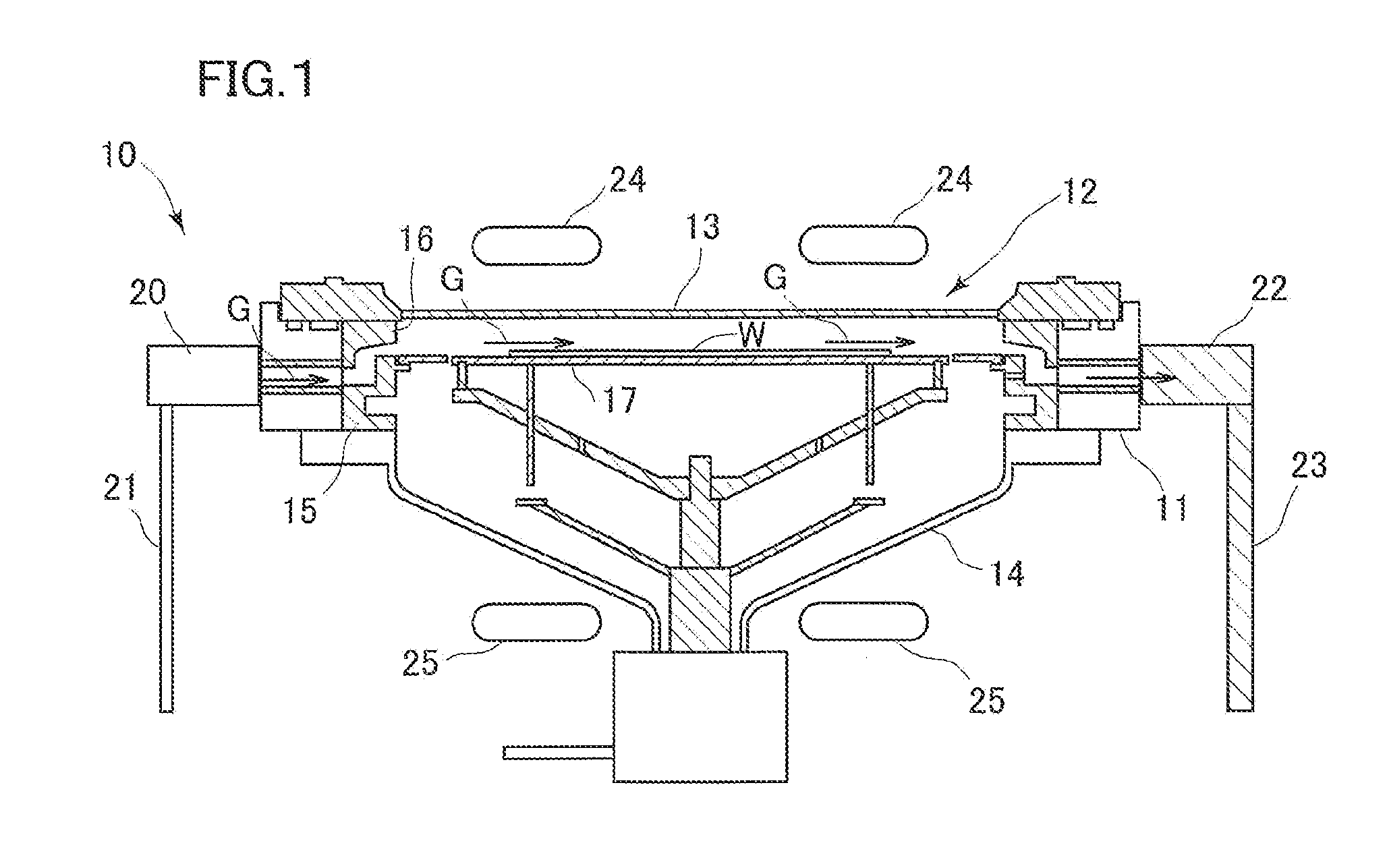
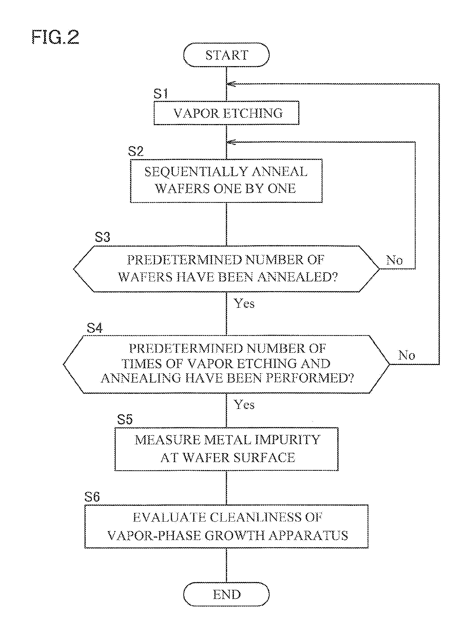
[0047]After maintenance of a vapor phase growth apparatus, when about 1000 silicon epitaxial wafers having a diameter of 300 mm had been manufactured, a chamber was subjected to vapor etching (VE) using HCl gas, and immediately thereafter, a silicon wafer was put in the chamber and annealed in H2 atmosphere at 1130° C. for 60 seconds. After the wafer was taken out, a second wafer was put in the chamber, subjected to the same annealing as above, and taken out. Further, a third wafer was put in the chamber, subjected to the same annealing as above, and taken out. Then, contamination at the surface of each wafer was collected, and the Mo concentration was measured by ICP-MS. Subsequently, the same VE as above was performed. Thereafter, the same three wafers as above were sequentially put in the chamber in the same order as above, and subjected to the same annealing as above. The vapor etching step and the annealing step were repeated up to four times in total. After the second and the ...
example 2
[0051]An experiment similar to Example 1 was conducted. However, in Example 2, a part within a radius of 85 mm of a silicon epitaxial wafer having a diameter of 300 mm was regarded as an inner circumference part (refer to FIG. 5), and a part corresponding to 65 mm from the radius of 85 mm to 150 mm (outermost periphery) of the silicon epitaxial wafer was regarded as an outer circumference part (refer to FIG. 5). The number of repetition of VE and annealing was four. The inner circumference part and the outer circumference part of each of three wafers were compared for the Mo concentration. FIG. 6 shows the result of the measurement. As shown in FIG. 6, in each of the first, second, and third wafers, the Mo concentration of the outer circumference part is higher than the Mo concentration of the inner circumference part. The outer circumference part is usually more contaminated than the inner circumference part, and the same result as usual is achieved.
example 3
[0052]After maintenance of a vapor phase growth apparatus, the same VE and annealing as those of Example 1 were performed four times and comparison of Mo concentrations was performed, at a time when 133 silicon epitaxial wafers having a diameter of 300 mm had been manufactured, at a time when 1401 silicon epitaxial wafers had been manufactured, and at a time when 2266 silicon epitaxial wafers had been manufactured. FIG. 7 shows the result of the measurement. FIG. 7 also shows the resultant WLTs. As shown in FIG. 7, the lesser the number of wafers manufactured after the maintenance is, the higher the Mo concentration is in order of the first wafer, the second wafer, and the third wafer. The difference in the Mo concentrations is more prominent as compared to the difference in the WLTs. However, after 2266 wafers had been manufactured, contamination due to the maintenance seemed to be removed by evacuation or the like, and FIG. 7 shows that the Mo concentrations of the first to third ...
PUM
| Property | Measurement | Unit |
|---|---|---|
| diameter | aaaaa | aaaaa |
| temperature | aaaaa | aaaaa |
| temperature | aaaaa | aaaaa |
Abstract
Description
Claims
Application Information
 - R&D
- Intellectual Property
- Life Sciences
- Materials
- Tech Scout
- Unparalleled Data Quality
- Higher Quality Content
- 60% Fewer Hallucinations
Browse by: Latest US Patents, China's latest patents, Technical Efficacy Thesaurus, Application Domain, Technology Topic, Popular Technical Reports.
© 2025 PatSnap. All rights reserved.Legal|Privacy policy|Modern Slavery Act Transparency Statement|Sitemap|About US| Contact US: help@patsnap.com