Method for manufacturing semiconductor device
a manufacturing method and semiconductor technology, applied in the direction of transistors, electroluminescent light sources, electric lighting sources, etc., can solve the problems of poor electrical characteristics of transistors, and achieve the effect of improving the electrical characteristics improving the reliability of a semiconductor device using an oxide semiconductor
- Summary
- Abstract
- Description
- Claims
- Application Information
AI Technical Summary
Benefits of technology
Problems solved by technology
Method used
Image
Examples
embodiment 1
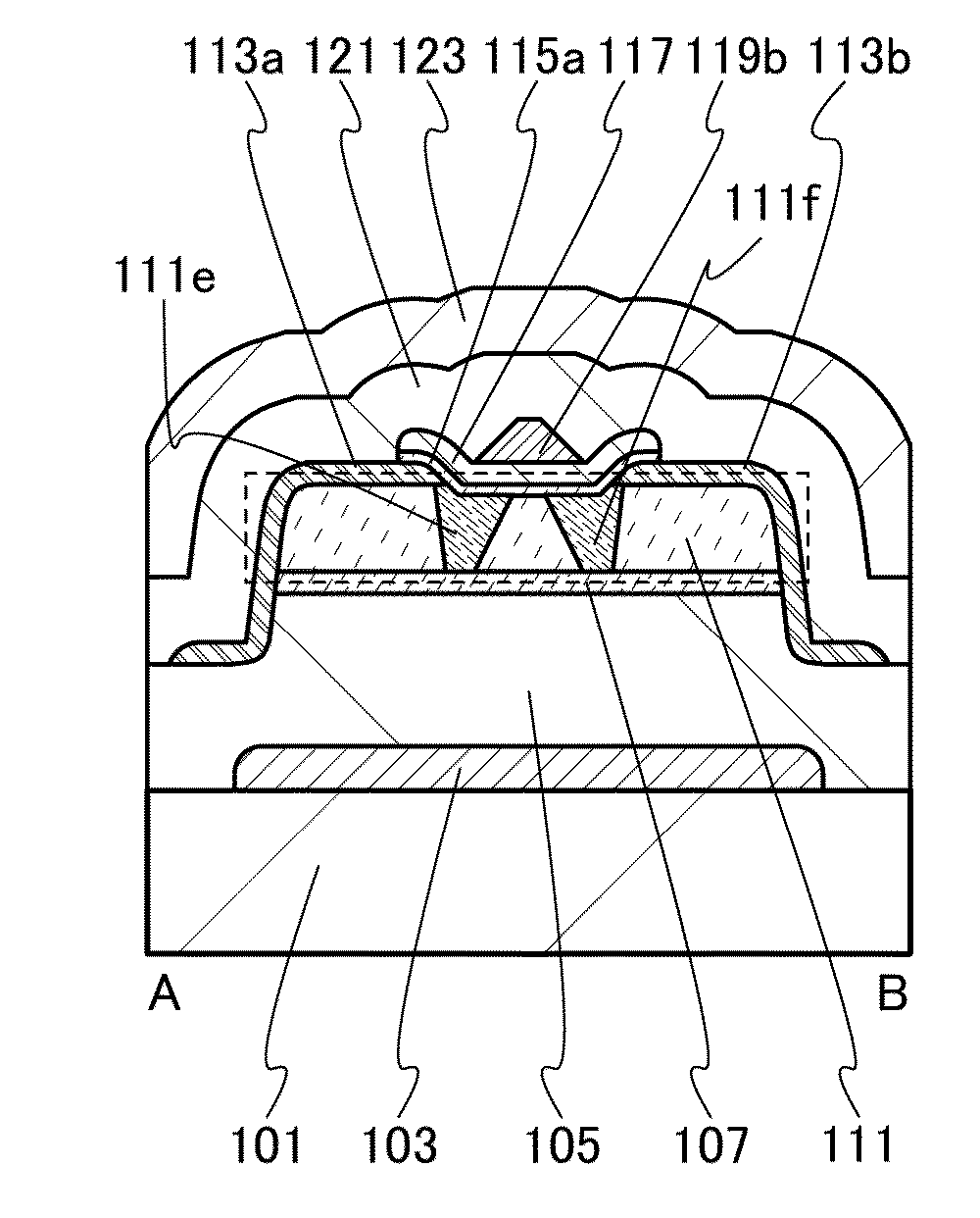
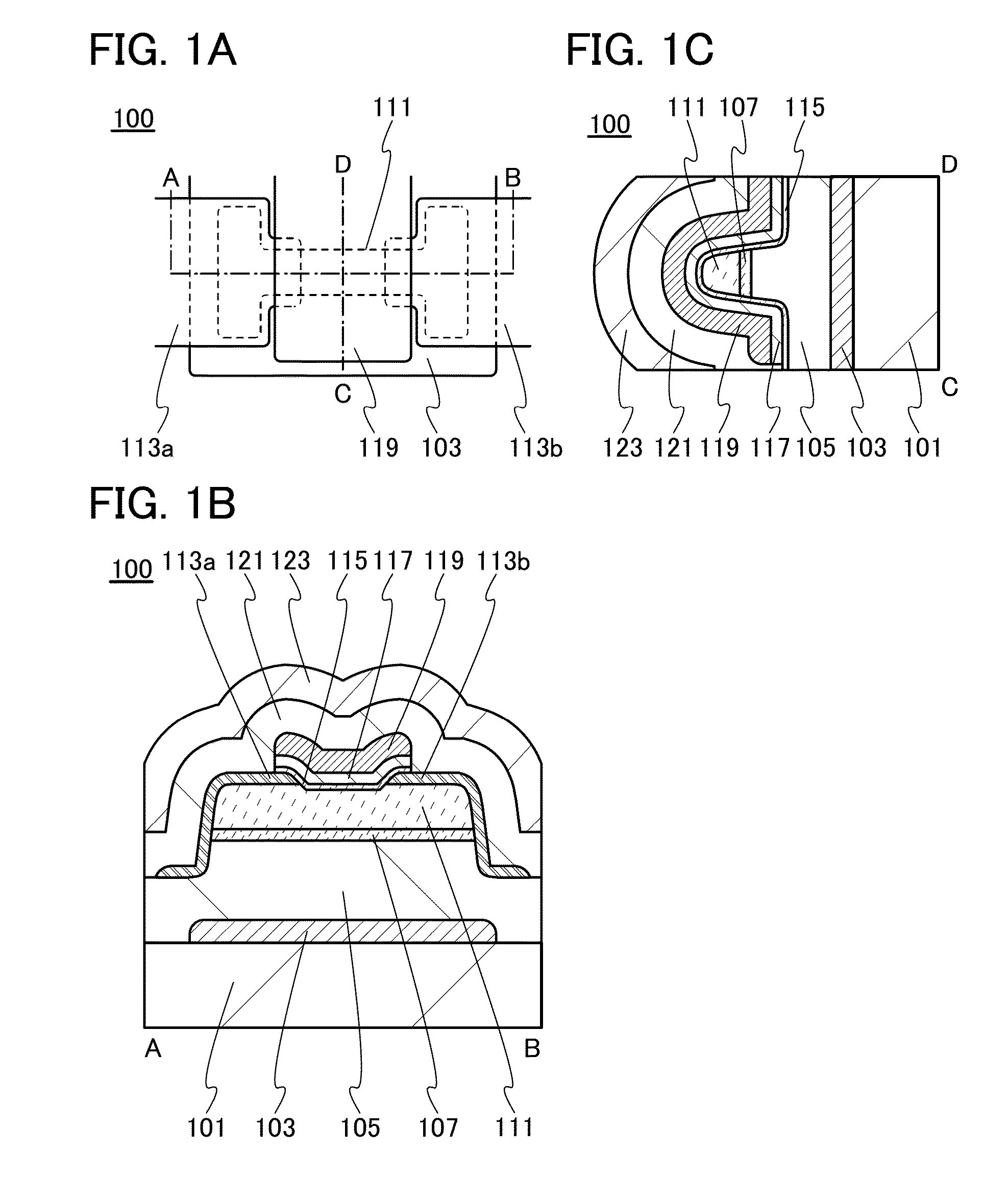
[0076]The threshold voltage of a transistor using an oxide semiconductor film with oxygen vacancies easily shifts in the negative direction, and such a transistor tends to be normally-on. This is because electric charges are generated owing to oxygen vacancies in the oxide semiconductor, and the resistance is reduced. In addition, a transistor using an oxide semiconductor film with oxygen vacancies has such a problem that the electrical characteristics, typically, the threshold voltage, are changed with time or changed by a stress test (typically, a gate bias-temperature (BT) stress test under light irradiation). In this embodiment, a highly reliable semiconductor device in which a change in threshold voltage is small and a manufacturing method thereof will be described. Further, a semiconductor device with excellent electrical characteristics and a manufacturing method thereof will be described.
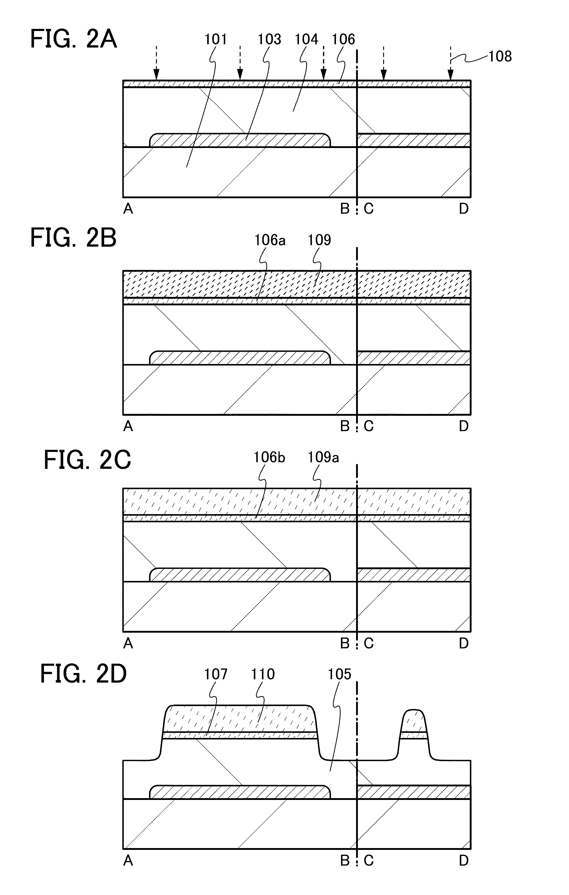
[0077]In this embodiment, a method for manufacturing a top-gate transistor is described....
embodiment 2
[0285]In this embodiment, a method for reducing oxygen vacancies in an oxide semiconductor film, which is different from the method in Embodiment 1, will be described. This embodiment is different from Embodiment 1 in adding oxygen to an oxide semiconductor film positioned over the pair of electrodes 113a and 113b.
[0286]As illustrated in FIG. 10A, the gate electrode 103 is formed over the substrate 101, and the insulating film 104 is formed over the gate electrode 103. Then, the oxide semiconductor film 106 is formed over the insulating film 104, and the oxide semiconductor film 109 is formed over the oxide semiconductor film 106.
[0287]Next, a mask is formed over the oxide semiconductor film 109 by a lithography process, and part of the insulating film 104, part of the oxide semiconductor film 106, and part of the oxide semiconductor film 109 are etched using the mask; thus, the gate insulating film 105, the oxide semiconductor film 107, and an oxide semiconductor film 110a are for...
embodiment 3
[0309]Transistors each having a stacked structure of oxide semiconductor films different from that of the transistor 100 illustrated in FIGS. 1A to 1C will be described with reference to FIGS. 13A to 13C.
[0310]A transistor 100f illustrated in FIG. 13A is different from the transistor 100 illustrated in FIG. 1B in not including the oxide semiconductor film 115. In other words, the transistor 100f is characterized by including the gate insulating film 117 that is in contact with the oxide semiconductor film 111, the pair of electrodes 113a and 113b, and the gate electrode 119.
[0311]Note that in a method for manufacturing the transistor 100f illustrated in FIG. 13A, the method for forming the oxide semiconductor film 111 described in Embodiment 1 can be used as appropriate.
[0312]A transistor 100g illustrated in FIG. 13B is different from the transistor 100 illustrated in FIG. 1B in not including the oxide semiconductor film 107. In other words, the transistor 100g is characterized by i...
PUM
 Abstract
Description
Claims
Application Information
 - R&D
- Intellectual Property
- Life Sciences
- Materials
- Tech Scout
- Unparalleled Data Quality
- Higher Quality Content
- 60% Fewer Hallucinations
Browse by: Latest US Patents, China's latest patents, Technical Efficacy Thesaurus, Application Domain, Technology Topic, Popular Technical Reports.
© 2025 PatSnap. All rights reserved.Legal|Privacy policy|Modern Slavery Act Transparency Statement|Sitemap|About US| Contact US: help@patsnap.com


