
Signal sectioning for profiling printed-circuit-bord vias with vertical scanning interferometry

Active Publication Date: 2015-04-16
BRUKER NANO INC
View PDF5 Cites 10 Cited by
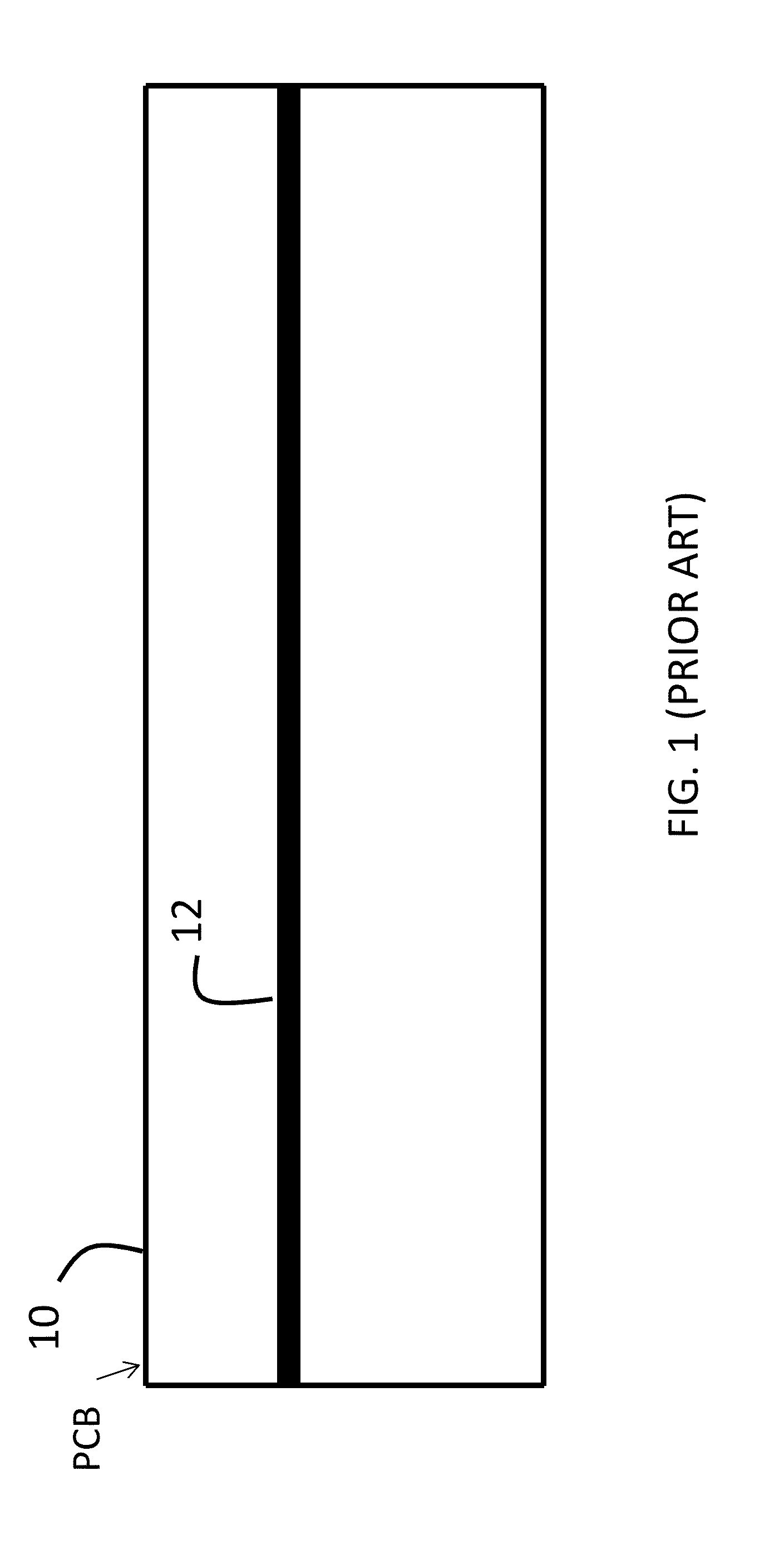
  • Summary
  • Abstract
  • Description
  • Claims
  • Application Information

AI Technical Summary

Benefits of technology

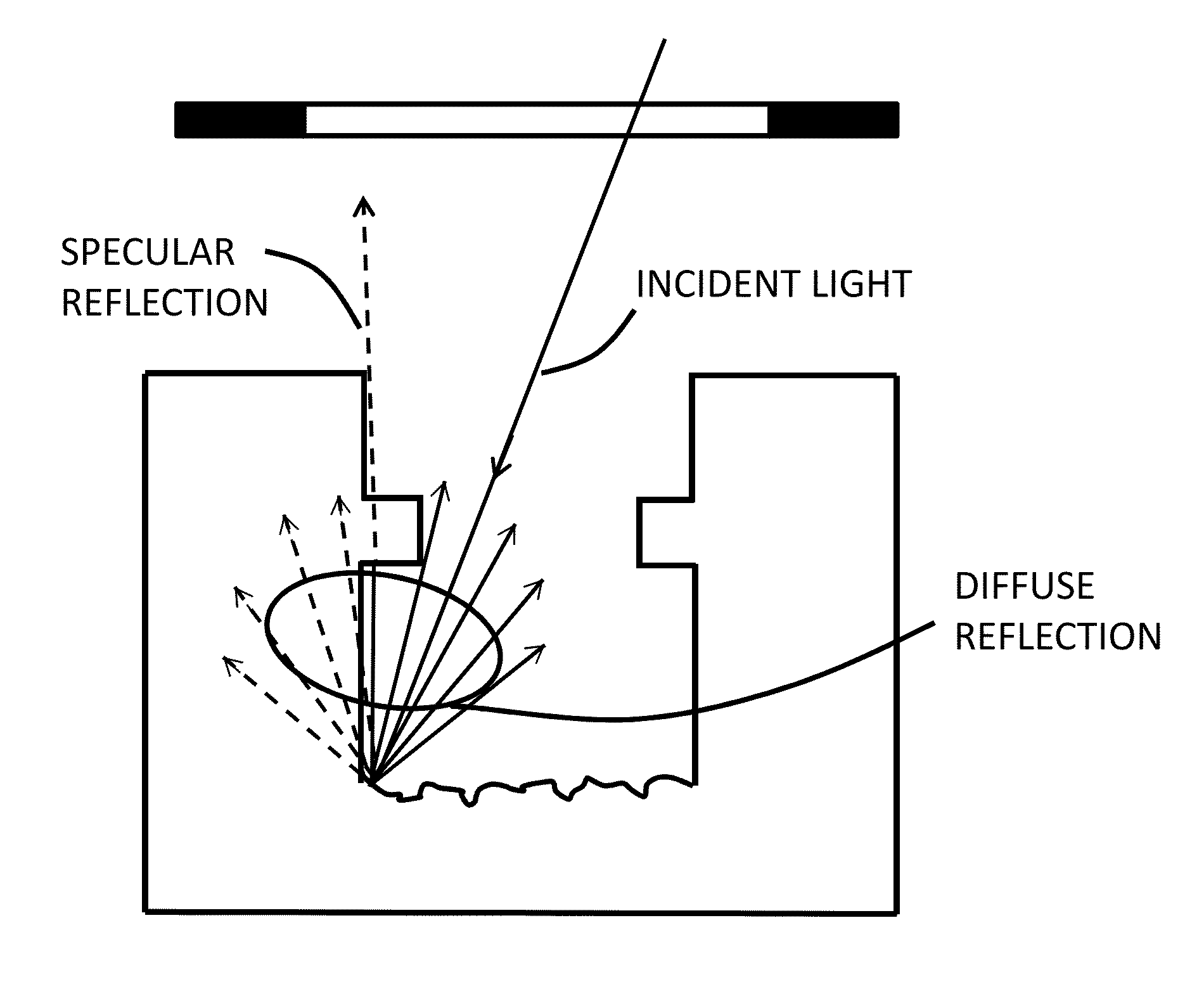
The invention is about a new method for measuring the surface of a fiber optic connector. This is important because the surface roughness of the connector can affect the amount of light that reflects back to the original source. By measuring the reflected light, the method can get more precise data about the bottom surface of the connector. The results can be used to make better quality fiber optic connections. The method uses a special laser technique to create a rough surface on the bottom of the connector, which scatters the reflected light and allows for the measurement of the entire surface. Rather than discarding the light from the surface of the connector, the method processes the light from the bottom to get a more accurate profile. This can be useful for improving the quality of fiber optic connections.

Problems solved by technology

This is contrary to expectation because scanning interferometry is based on interference between a reference beam and a sample beam reflected from the surface being measured.

Method used


Image

  • Signal sectioning for profiling printed-circuit-bord vias with vertical scanning interferometry
  • Signal sectioning for profiling printed-circuit-bord vias with vertical scanning interferometry
  • Signal sectioning for profiling printed-circuit-bord vias with vertical scanning interferometry

Examples


Embodiment Construction

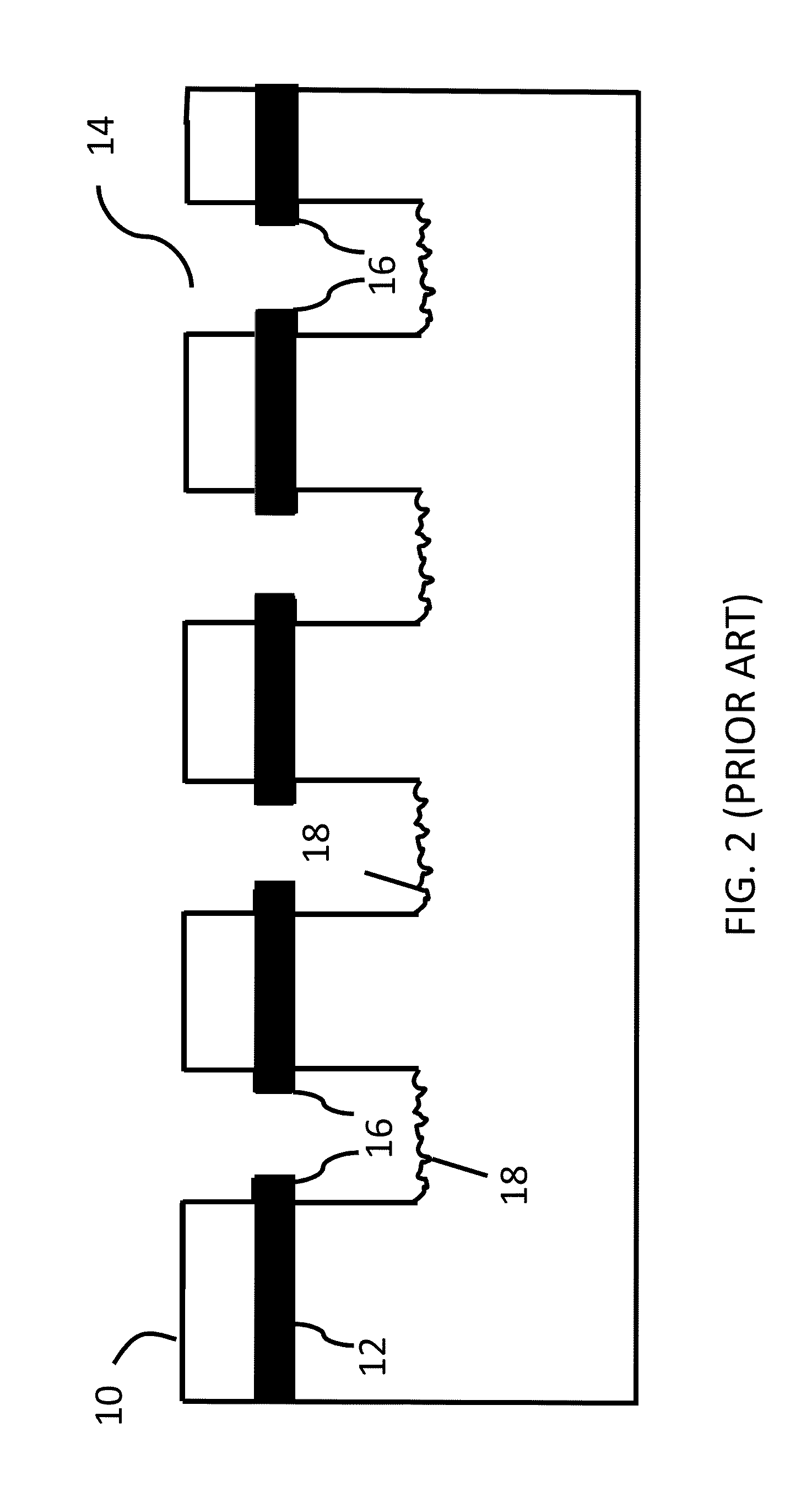
[0029]As used herein, the term “shelf” refers to the substantially annular structure of reinforcing fibers produced by the process of forming a via in a printed circuit board. As a result of the different materials constituting the reinforcing fibers and the rest of the PCB, the bottom surface of the via includes a correspondingly annular area that is obscured by the overlying fiber shelf and not directly visible from the top opening of the via. The terms “diffused” and “scattered” and their derivatives are used synonymously.

[0030]The invention is described below with reference to low-coherence interferometry (normally referred to in the art also as low-coherence white light interferometry—WLI—or vertical scanning interferometry—VSI). However, it is recognized that it is applicable to any through-focus optical method of measurement. Therefore, for the purposes of claiming the invention, the term “through-focus” is intended to encompass any optical approach whereby an optical signal ...


PUM

PropertyMeasurementUnit
Surface roughnessaaaaaaaaaa
Diameteraaaaaaaaaa
Surface roughnessaaaaaaaaaa

Abstract

The rough bottom surface of a recessed feature partially obscured by an overlying structure is profiled interferometrically with acceptable precision using an objective with sufficiently large numerical aperture to illuminate the bottom under the obscuring structure. The light scattering produced by the roughness of the surface causes diffused light to return to the objective and yield reliable data fringes. Under such appropriate numerical-aperture and surface roughness conditions, the bottom surface of such recessed features can be profiled correctly simply by segmenting the correlograms produced by the scan and processing all fringes that correspond to the bottom surface elevation.

Description

RELATED APPLICATIONS[0001]This application is a continuation-in-part application of U.S. Ser. No. 13 / 719,101, filed Dec. 18, 2012.BACKGROUND OF THE INVENTION[0002]1. Field of the Invention[0003]This invention pertains to the general field of optical metrology. In particular, the invention relates to a method for profiling the bottom surface of vias in printed circuit boards when the view is partially obscured by preferentially oriented reinforcement fibers added to the structure of the boards.[0004]2. Description of the Prior Art[0005]Printed circuit boards (PCBs) are well known structures used in the electronic industry to mount electronic components and connect them to external devices. Printed circuit boards have traditionally been manufactured from fiber layers surrounded by a plastic matrix material. The boards have one or more layers of metalized patterns that, when assembled with the electronic components, form electrical interconnections among them.[0006]In use, assembled PC...

Claims


Application Information

Patent Timeline
IPC IPC(8): G01B11/24
CPCG01B11/2441G01B11/303G01B2210/56G01N21/954G01N2021/95653H05K1/0366H05K3/0035
Inventor SCHMIT, JOANNANOVAK, ERIK
Owner BRUKER NANO INC
Learn More