Printed circuit board and method of manufacturing the same

a technology of printed circuit boards and manufacturing methods, applied in the direction of cable/conductor manufacturing, printed element electric connection formation, dielectric characteristics, etc., can solve the problems of dimple generation, long signal processing time, thick core board thickness, etc., and achieve the effect of preventing dimple generation

Inactive Publication Date: 2015-04-16
SAMSUNG ELECTRO MECHANICS CO LTD
View PDF6 Cites 4 Cited by
  • Summary
  • Abstract
  • Description
  • Claims
  • Application Information

AI Technical Summary

Benefits of technology

The present invention aims to provide a printed circuit board that can prevent the generation of dimples and a method of manufacturing it. Additionally, the invention seeks to create a printed circuit board that can have a via formed on its circuit pattern to prevent it from being lost during an etching process and a method of manufacturing it.

Problems solved by technology

However, a thickness of the core board is thick and a signal processing time thereof is long.
In addition, as electronic products such as a smart device, and the like, become thin, thinness of products mounted therein has also been required.

Method used


Image

  • Printed circuit board and method of manufacturing the same
  • Printed circuit board and method of manufacturing the same
  • Printed circuit board and method of manufacturing the same

Examples


Embodiment Construction

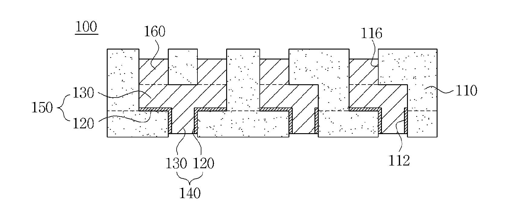
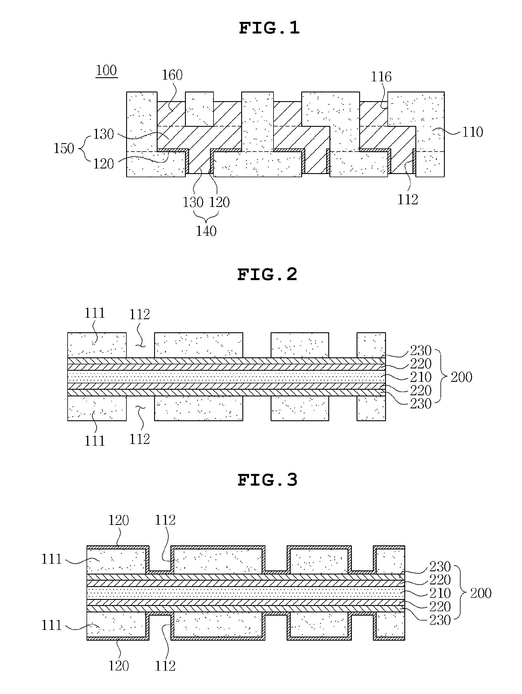
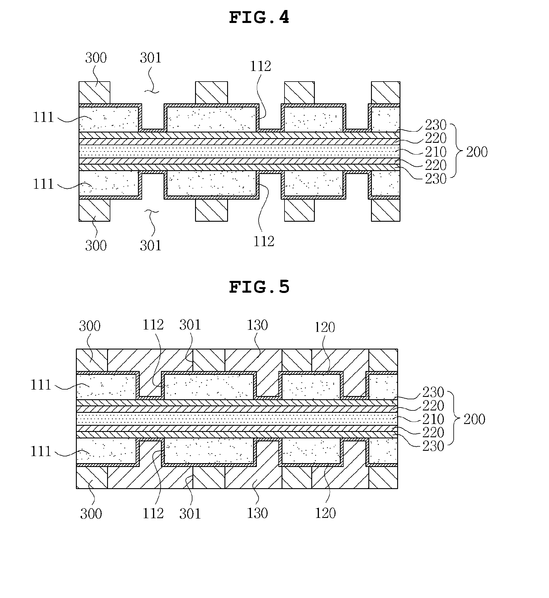
[0032]The objects, features and advantages of the present invention will be more clearly understood from the following detailed description of the preferred embodiments taken in conjunction with the accompanying drawings. Throughout the accompanying drawings, the same reference numerals are used to designate the same or similar components, and redundant descriptions thereof are omitted. Further, in the following description, the terms “first”, “second”, “one side”, “the other side” and the like are used to differentiate a certain component from other components, but the configuration of such components should not be construed to be limited by the terms. Further, in the description of the present invention, when it is determined that the detailed description of the related art would obscure the gist of the present invention, the description thereof will be omitted.

[0033]Hereinafter, preferred embodiments of the present invention will be described in detail with reference to the attac...


PUM

PropertyMeasurementUnit
Thicknessaaaaaaaaaa
Electrical conductoraaaaaaaaaa
Depthaaaaaaaaaa

Abstract

Disclosed herein are a printed circuit board and a method of manufacturing the same.The printed circuit board according to a preferred embodiment of the present invention may include: an insulating layer; a first via depressed from one surface of the insulating layer; a second via depressed from the other surface of the insulating layer; and a circuit pattern formed in the insulating layer and bonded to the first and second vias.

Description

CROSS REFERENCE TO RELATED APPLICATION[0001]This application claims the benefit of Korean Patent Application No. 10-2013-0122126, filed on Oct. 14, 2013, entitled “Printed Circuit Board and Method of Manufacturing the Same”, which is hereby incorporated by reference in its entirety into this application.BACKGROUND OF THE INVENTION[0002]1. Technical Field[0003]The present invention relates to a printed circuit board and a method of manufacturing the same.[0004]2. Description of the Related Art[0005]Recently, a trend of multifunctional and high-speed electronic products has rapidly progressed. In order to cope with this trend, a semiconductor chip and a printed circuit board mounted with the semiconductor chip have also been very rapidly developed. In the printed circuit board as described above, slimness and lightness, a fine circuit, excellent electric properties, high reliability, and high-speed signal transferring, and the like, are required.[0006]According to the prior art, a cor...

Claims


Application Information

Patent Timeline
IPC IPC(8): H05K1/11H05K3/04H05K1/09
CPCH05K1/115H05K1/092H05K3/048H05K2201/0104H05K2201/09818H05K2201/09563H05K3/0097H05K3/108H05K3/426H05K3/428H05K3/465H05K2201/0347H05K2201/09472H05K2201/09545H05K2203/1536Y10T29/49165H05K1/02H05K3/40
Inventor PARK, JONG TAEKANG, HO SHIK
Owner SAMSUNG ELECTRO MECHANICS CO LTD
Why Eureka
Try Eureka