Semiconductor device and internal combustion engine ignition device
a technology of semiconductor elements and ignition devices, which is applied in the direction of ignition safety means, machines/engines, pulse techniques, etc., can solve the problems of difficult to keep balance in the control circuit, the size of the semiconductor element cannot be reduced, and the achievement of low resistance cannot lead to cost reduction, etc., to achieve small control circuits, simple control circuits, and elimination of feedback loops
- Summary
- Abstract
- Description
- Claims
- Application Information
AI Technical Summary
Benefits of technology
Problems solved by technology
Method used
Image
Examples
embodiment 1
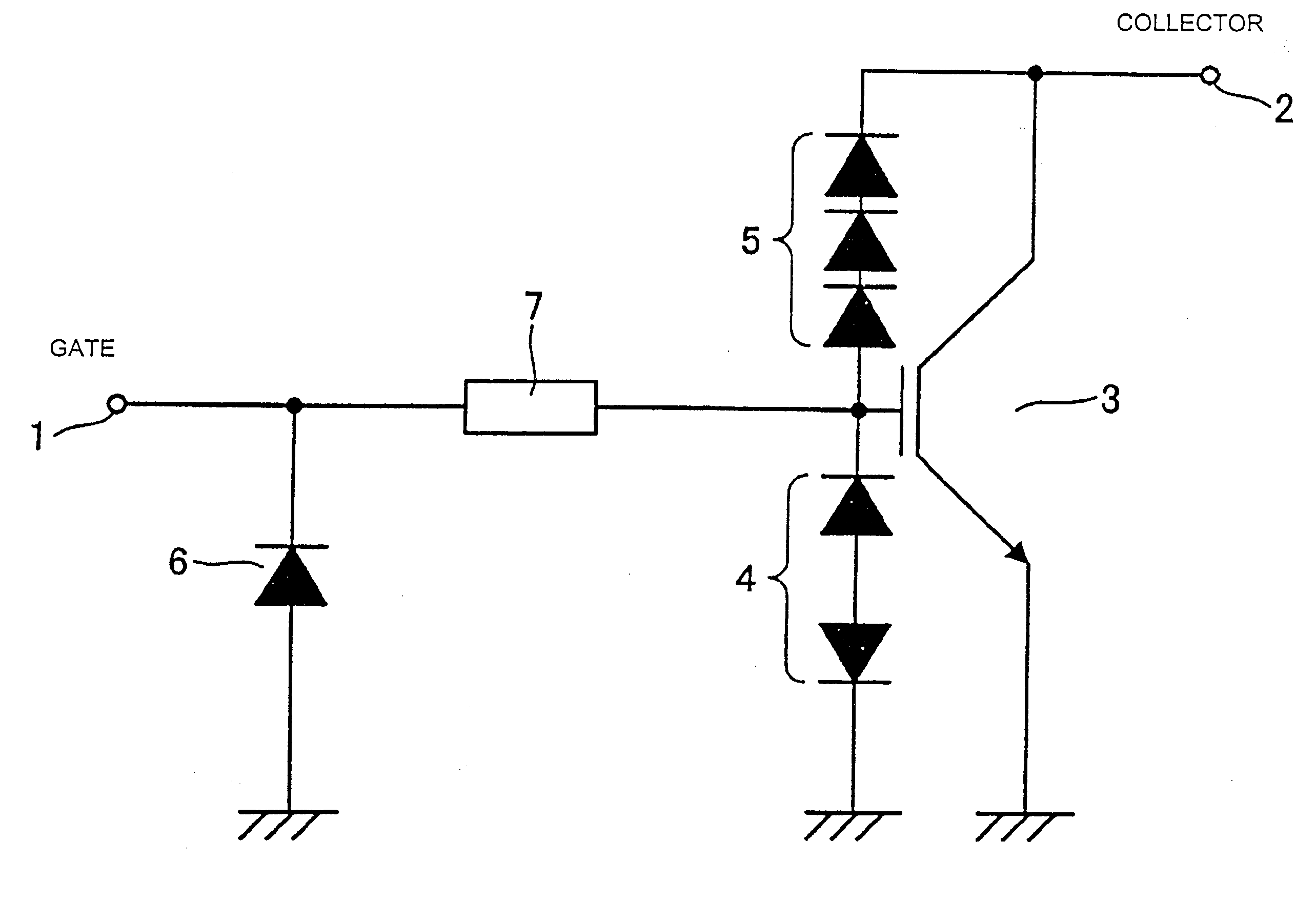
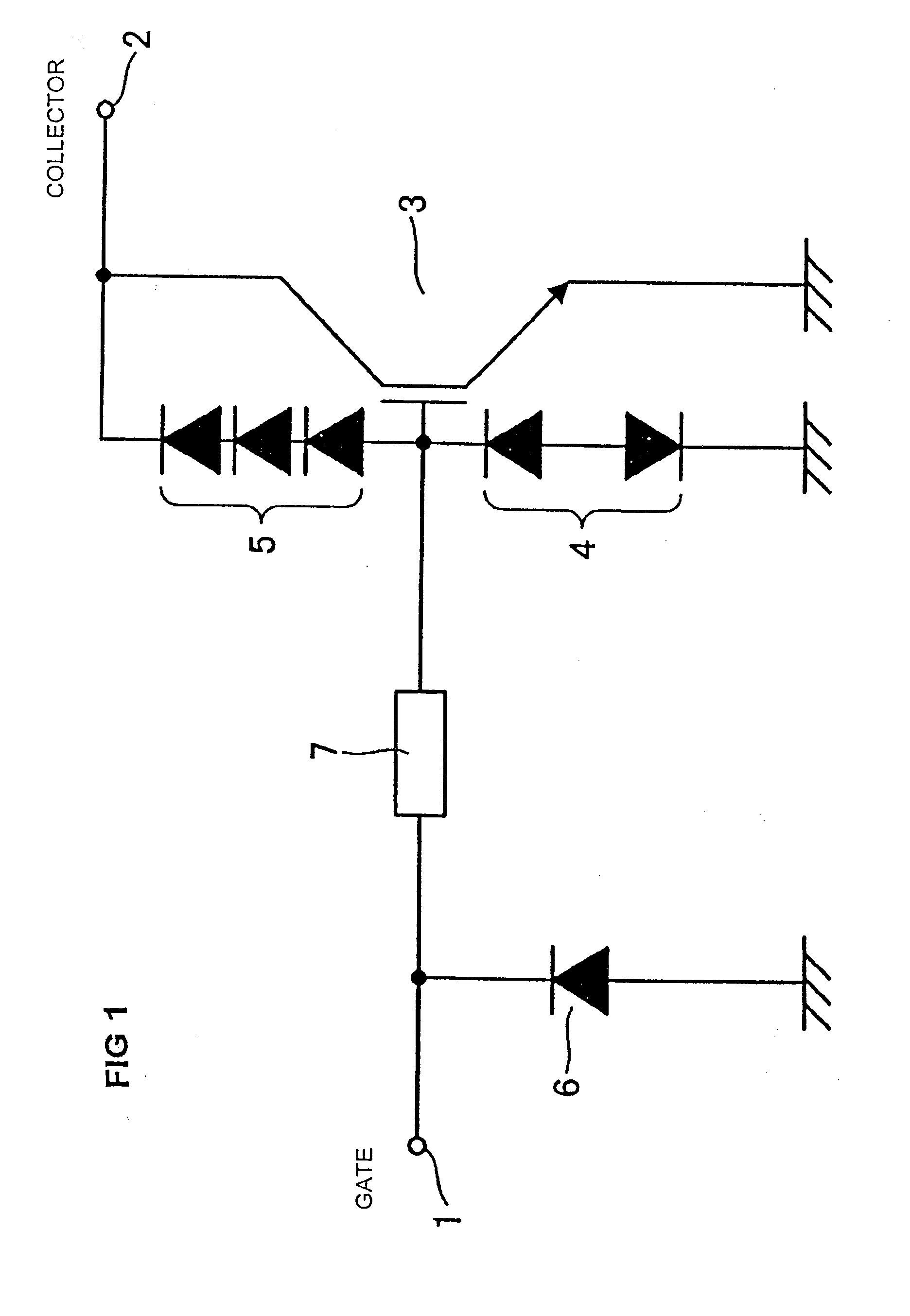
[0056]An emitter resistor may be provided between the emitter of the IGBT 3 and the ground. FIG. 3 is a circuit diagram showing another example of the semiconductor switch having the constant voltage circuit according to The semiconductor switch is additionally provided with an emitter resistor 8. When a saturation current flows into the IGBT 3, a practically effective gate voltage of the IGBT 3 decreases due to voltage drop of the emitter resistor 8 so that the saturation current of the IGBT 3 decreases. When a current in a normal operation range flows into the IGBT 3, the voltage drop of the emitter resistor 8 is small so that the influence of the emitter resistor 8 on an on-voltage becomes small. The reason will be described later.
[0057]Since a current flowing in the IGBT 3 decreases in accordance with temperature rise of the IGBT 3 in a saturation region, the constant voltage circuit 7 may be provided with a function of increasing the gate voltage in accordance with the tempera...
embodiment 4
[0070]As described above, since the IGBT 33 and the control circuit 32 are formed separately on different semiconductor substrates , the IGBT 33 and the control circuit 32 can be produced in the most suitable manufacturing processes respectively. Therefore, high-level control suitable for the IGBT 33 and the control circuit 32 can be performed.
[0071]FIG. 8 is a sectional view showing a semiconductor device in which resistors are built in an IGBT. In Embodiment 5, emitter resistors are formed in a planar gate type IGBT. As shown in FIG. 8, similarly to the planar gate type IGBT (see FIG. 5) in Embodiment 3, an n+ buffer layer 42 and an n drift layer 43 are formed on a front surface of a p+ collector layer 41 and two p base regions 44 are provided separately in parts of a front surface of the n drift layer 43. A p+ contact region 45 is provided in part of a front surface of the n drift layer 43 so as to be adjacent to the two p base regions 44. An n+ resistance region 46 is provided i...
embodiment 5
[0086]FIG. 17 shows the relation between an on-voltage and a saturation current with / without emitter resistors in a planar gate structure IGBT and a trench gate structure IGBT. It is found from the results of FIG. 17 that trade-off characteristic between the on-voltage and the saturation current value is further improved when the emitter resistors are provided. It is found that the planar gate structure IGBT is further improved in the trade-off characteristic between the on-voltage and the saturation current value when the emitter resistors are formed in source regions of the IGBT (“planar with emitter resistors in source regions” shown in FIG. 17), similarly to the semiconductor device according to
[0087]A practically effective gate voltage applied to the IGBT is a voltage difference between the gate voltage and the emitter voltage of the IGBT. For this reason, in the case where the emitter resistors are provided, the voltage of each emitter resistor drops largely in accordance with...
PUM
 Abstract
Description
Claims
Application Information
 - Generate Ideas
- Intellectual Property
- Life Sciences
- Materials
- Tech Scout
- Unparalleled Data Quality
- Higher Quality Content
- 60% Fewer Hallucinations
Browse by: Latest US Patents, China's latest patents, Technical Efficacy Thesaurus, Application Domain, Technology Topic, Popular Technical Reports.
© 2025 PatSnap. All rights reserved.Legal|Privacy policy|Modern Slavery Act Transparency Statement|Sitemap|About US| Contact US: help@patsnap.com


